Electronic Components blog
Thursday, june 14, 2012, 400w power amplifier "safari" circuit diagram.

This can made 40 W but 400 w never

- Tone Control
- Science Projects

500W Power Amplifier Circuit using c5200 a1943
Introduction.
Power amplifiers are essential components of audio systems since they amplify the low-level signals to high levels to drive speakers. A 500W power amplifier circuit is an ideal design for these applications. This kind of amplifier makes it possible for the system to produce sound that is loud enough to be heard in large spaces. This article will discuss the 500W power amplifier circuit using 5 x 2SC5200 , 5 x 2SA1943 , D718 , B688 , TIP42 , A1015 and C1815 transistors.
The amplifier circuit uses five pairs of 2SC5200 and 2SA1943 power transistors. Each pair of transistors is connected in a push-pull configuration . The push-pull configuration provides a higher power output than the common emitter configuration that is generally used in small scale amplifiers .
Circuit Diagram
Of 500w power amplifier circuit.
This amplifier can be designed using a few basic components. The circuit diagram of this project is shown below.

NOTE: Correction of R26 (150 ohm) connected from emitter to collector of Q9 (C2229), will be connected from emitter to -75VDC.

More Circuit Layouts
Explanation of 500W Power Amplifier Circuit
The transistors used in this amplifier circuit are known for their high current gain , high power handling capability and thermal stability . The transistors D718 and B688 are used as drivers to drive the output transistors. These drivers have enough current capability to drive the base of the output transistors .
The amplifier circuit has a power supply section that provides the required DC voltage to operate the amplifier. The power supply uses a low-loss rectifier with a filter capacitor that provides a stable DC voltage .
Conclusion of 500W Power Amplifier Circuit
The power amplifier circuit using 5 x 2SC5200, 5 x 2SA1943, D718, B688 transistors is an excellent choice for applications that require high power output . The amplifier can drive large speakers with ease and provide excellent sound quality. The amplifier circuit is built using high-quality components that provide excellent thermal stability , which is essential for power amplifiers .
The use of five pairs of transistors in a push-pull configuration ensures that the amplifier has a high output power. The drivers used in the circuit have an adequate current capability to drive the transistors’ base, thereby ensuring that the transistors operate in their active region.
In conclusion, the power amplifier circuit 2SC5200, 2SA1943 transistors provides excellent sound quality and high power output, making it an ideal choice for audio applications that require high-quality sound.
More projects, You may like:
- Video Transmitter DIY Homemade FM Radio Transmitter
- Adjustable Power Supply DIY Battery Charger
- 12V-220V 500 Watt inverter DIY Homemade
- 12V-220V H-Bridge Inverter DIY Homemade
- MPPT Solar Charge Controller DIY Homemade
- 18650 battery bank free charge protection module
- D718 B688 Bass Amplifier Homemade DIY
- C5200 Bass Amplifier DIY Homemade with Volume
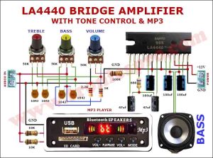
- DIY LA4440 bass amplifier homemade
- C5200 A1943 TDA2030 Amplifier DIY Homemade
For more project and circuit diagrams, you can go through the Schematics in the main menu where you can find many interesting projects and circuit diagrams like audio amplifier circuits , voltage booster circuit , battery charger circuit and timer circuits etc., which are all beginner circuit projects . Feel free to check them out!
You may also like:

5 comments on 500W Power Amplifier Circuit using c5200 a1943
Muito bom e objetivo o assunto amigo profissional..!
Muito obrigado amigo!
We buy kit power amp, 50w, 100w 200w 400w 500w 100w
Sorry we don’t sell here.
Hello, I would be extremely grateful if someone could send me this diagram as a document, not as a picture, ideal for finishing so that I don’t have to redraw the whole thing
Leave a Reply Cancel reply
Your email address will not be published. Required fields are marked *
Save my name, email, and website in this browser for the next time I comment.
Search for Electronics Projects
Popular posts.

- Amplifiers (38)
- Bass Treble Controllers (7)
- Circuit Diagrams (327)
- Circuit Layouts (28)
- Science Projects (5)
- Simple Electronics (132)
Recent Posts

Advertisement
- Terms and Conditions
- Privacy Policy

400W Power Amplifier “Safari”
400w power amplifier - safari.

About Circuit Gallery
Related posts, 0 comments:, post a comment.
- Evaluation Boards & Kits
- FPGA Reference Designs
- Quick Start Guides
- Linux Software Drivers
- Microcontroller Software Drivers
- ACE Software
- Technical Guides
- University Program Overview
- ADALM1000 (M1k) Active Learning Module
- ADALM2000 (M2k) Active Learning Module
- ADALP2000 Parts kit for Circuits
- ADALM-PLUTO SDR Active Learning Module
- Teaching and Lab Materials
- Wiki Site Map
- Recent Changes
- Media Manager
- Analog Devices Wiki

Table of Contents
9.1 basic amplifiers, 9.2.1 dc bias techniques, common emitter/source, 9.2.2 small signal voltage gain, common emitter or source, 9.2.3 small signal input impedance, common emitter or source, 9.2.4 small signal output impedance, common emitter or source, 9.2.5 common emitter and source lab activities, 9.3.1 dc biasing techniques, current follower or common base/gate amplifier, 9.3.2 small signal voltage gain, current follower or common base/gate amplifier, 9.3.3 input impedance, current follower or common base/gate amplifier, 9.3.4 output impedance, current follower or common base/gate amplifier, 9.4 voltage followers (also called emitter or source follower or common collector or drain amplifiers), 9.4.1 dc biasing techniques, voltage follower or common collector/drain amplifier, 9.4.2 voltage gain, common collector or drain amplifier, example 9.4.2 calculating the voltage gain, 9.4.3 input impedance, voltage follower (common collector or drain), 9.4.4 output impedance, voltage follower (common collector or drain), 9.4.5 voltage follower (common collector or drain) lab activities, 9.5.1 small signal voltage gain with emitter/source degeneration, 9.5.2 small signal input impedance with emitter/source degeneration, 9.5.3 small signal output impedance with emitter/source degeneration, 9.5.4 dc biasing techniques with emitter/source degeneration, 9.5.5 summary - performing small-signal analyses:, 9.6 miller’s theorem, 9.7.1 mos version, 9.7.2 bjt version dc biasing techniques, example 9.7.2 using miller’s theorem, exercise 9.7, 9.7.5 the miller effect, example 9.7.3 miller capacitance example, appendix: source absorption theorem, example a1: finding the emitter resistance using source absorption theorem, at1 diode bias generation, chapter 9: single transistor amplifier stages:.
The term amplifier as used in this chapter means a circuit (or stage) using a single active device rather than a complete system such as an integrated circuit operational amplifier. An amplifier is a device for increasing the power of a signal. This is accomplished by taking energy from a power supply and controlling the output to duplicate the shape of the input signal but with a larger (voltage or current) amplitude. In this sense, an amplifier may be thought of as modulating the voltage or current of the power supply to produce its output.
The basic amplifier, figure 9.1, has two ports and is characterized by its gain, input impedance and output impedance. An ideal amplifier has infinite input impedance (R in = ∞), zero output impedance (R out = 0) and infinite gain (A vo = ∞) and infinite bandwidth if desired.

Figure 9.1 Basic Amplifier Model
The transistor, as we have seen in the previous chapter, is a three-terminal device. Representing the basic amplifier as a two port network as in figure 9.1, there would need to be two input and two output terminals for a total of four. This means one of the transistor terminals must be common to both the input and output circuits. This leads to the names common emitter, etc. for the three basic types of amplifiers. The easiest way to determine if a device is connected as common emitter/source, common collector/drain, or common base/gate is to examine where the input signal enters and the output signal leaves. The remaining terminal is what is thus common to both input and output. In this chapter we will primarily be using n-type transistors (NPN, NMOS) in the example circuits. The same basic amplifier stages can just as easily be implemented using p-type transistors (PNP, PMOS). When larger multi-stage amplifiers are assembled, both types of transistors are often interspersed with each other.
Building-block amplifier stages:
- Inverting voltage amplifier (also called Common emitter or Common source amplifier)
- Current Follower (also called Common base or Common gate or cascode)
- Voltage Follower (also called Common collector or Common drain amplifier)
- Series feedback (more commonly: emitter/source degeneration)
- Shunt feedback
9.2 The inverting voltage amplifier or Common emitter/source
The common emitter/source amplifier is one of three basic single-stage amplifier topologies. The BJT and MOS versions function as an inverting voltage amplifier and are shown in figure 9.2. The base or gate terminal of the transistor serves as the input, the collector or drain is the output, and the emitter or source is common to both input and output (it may be tied to the ground reference or the power supply rail), which gives rise to its common name.

Figure 9.2: Basic n-type inverting voltage amplifier circuit (neglecting biasing details)
The common emitter or source amplifier may be viewed as a transconductance amplifier ( i.e. voltage in, current out) or as a voltage amplifier (voltage in, voltage out). As a transconductance amplifier, the small signal input voltage, v be for a BJT or v gs for a FET, times the device transconductance g m , modulates the amount of current flowing through the transistor, i c or i d . By passing this varying current through the output load resistance, R L it will be converted back into a voltage V out . However, the transistor’s small signal output resistance, r o , is not typically high enough for a reasonable transconductance amplifier (ideally infinite). Nor is the output load, R L , low enough for a decent voltage amplifier (ideally zero). Another major drawback is the amplifier’s limited high-frequency response due in part to the built in collector base or drain gate capacitance inherent to the transistor. More on how this capacitance effects the frequency response in a later section of this chapter. Therefore, in practice the output often is routed through either a voltage follower (common collector or drain stage), or a current follower (common base or gate stage), to obtain more favorable output and frequency characteristics. This latter combination is called a cascode amplifier as we will see later in the chapter on multi-stage amplifiers.
In comparison to the BJT common emitter amplifier, the FET common source amplifier has higher input impedance. The generally lower g m of the FET vs. the BJT at equal current levels leads to lower voltage gain for the MOS version.
In order for the common emitter or source amplifier to provide the largest output voltage swing, the voltage at the Base or Gate terminal of the transistor is offset in such a way that the transistor is nominally operating halfway between its cut-off and saturation points. Note the NMOS (a) and NPN (b) characteristic curves in figure 9.2.1. This allows the amplifier stage to more accurately reproduce the positive and negative halves of the input signal superimposed upon the DC Bias voltage. Without this offsetting Bias Voltage only the positive half of the input waveform would be amplified.

Figure 9.2.1 (a) I D vs. V DS curves and (b) I C vs. V CE curves
The red line superimposed on the two sets of curves represents the DC load line of a 400 ohm R L . To maximize the output swing it is desirable to set the operating point of the transistor, with a zero input signal, at a drain or collector voltage of one half the supply voltage, which would be 4 volts in this case. Finding the corresponding drain or collector current along the load line gives us the target current level. This is around 10mA for R L equal to 400 ohms. The next step is to determine the corresponding V GS or I B for a 10mA I D or I C . In the NMOS example each curve represents a different V GS from 0.9 volts to 1.5 volts in 0.1 volt steps. The NMOS device used in this example has a transconductance of about 40mA/ V . The I D equal to 10mA point on the load line falls between the 1.4V and 1.3V curves or a V GS of 1.32V. In the NPN example each curve represents a different I B from 10uA to 100uA in 10uA steps. The 50uA curve happens to cross the load line at I C =10mA. The β of the transistor must therefore be about 200. The task now is to somehow provide this DC offset or bias at the Gate or Base of the transistor.
The first bias technique we will explore is called voltage divider bias and is shown in figure 9.2.2. If we choose the correct resistor values for R 1 and R 2 that will result in a collector or drain current such that one half of the supply voltage, V + appears across R L we should have our desired value of V GS or V BE (I B ) for biasing with no signal input. For the MOS case we know that no current flows into the gate so the simple voltage divider ratio can be used to pick R 1 and R 2 . If V + = 8V and we want V GS to equal 1.32 V then:

The actual values of R 1 and R 2 are not so important just their ratio. However, the divider ratio we choose will be correct for only one set of conditions of power supply voltage, transistor threshold voltage and transconductance, and temperature. Actual designs often use more involved bias schemes.

Figure 9.2.2 Voltage divider bias
For the NPN case the calculation is somewhat more involved. We know we want I B to be equal to 50uA. The current that flows in R 1 is the sum of the current in R 2 and I B which puts an upper bound on R 1 when R 2 is infinite and no current flows in R 2 . If we assume a nominal V BE of 0.65 volts then R 1 must be no larger than 7.35V/50uA or 147KΩ. The purpose of the voltage divider is to attenuate the variations in V + and thus make the DC operating point of the transistor less sensitive to V +. To that end we need to make the current in R 2 many times larger than I B . If we, for example, choose to make I R2 9 times I B then the current in R 1 will be 10*I B or 500uA. R 1 will be 1/10 what we just calculated as the upper bound or 14.7KΩ. R 2 will be V BE divided by 450uA or 1.444KΩ which is a divider ratio of 0.8921. If we had simply used 8V- V BE /8V as the ratio (assume V BE = 0.65V) the divider ratio would have been 0.8125. Taking I B into account shifted the required ratio. These values would need to be adjusted slightly if the actual V BE was not the 0.65 volts (or β was not 200) we used in this calculation. This points out a major limitation of this bias scheme as we pointed out in the MOS example above. That is the sensitivity to device specific characteristics like V BE and β as well as supply voltage and temperature.
A consequence of including this bias scheme is a lowering of the input impedance. The input now includes the parallel combination of R 1 and R 2 across the input. For the MOS case this now sets the input resistance. For the BJT case we now have R 1 ||R 2 ||r π as the effective input resistance.
There is another minor inconvenient problem with this bias scheme when it is connected to a prior stage in the signal path. This bias configuration places the AC input signal source directly in parallel with R 2 of the voltage divider. This may not be acceptable, as the input source may tend to add or subtract from the DC voltage dropped across R 2 .
One way to make this scheme work, although it may not be obvious why it will work, is to place a coupling capacitor between the input voltage source and the voltage divider as in figure 9.2.3 below.

Figure 9.2.3 Coupling capacitor C C prevents voltage divider bias current from flowing into the input signal source.
The capacitor forms a high-pass filter between the input source and the DC voltage divider, passing almost the entire AC portion of the input signal on to the transistor while blocking all the DC bias voltage from being shorted through the input signal source. This makes much more sense if you understand the superposition theorem and how it works. According to superposition, any linear, bilateral circuit can be analyzed in a piecemeal fashion by only considering one power source at a time, then algebraically adding the effects of all power sources to find the final result. If we were to separate the capacitor and the R 1 /R 2 voltage divider circuit from the rest of the amplifier, it might be easier to understand how this superposition of AC and DC would work.
With only the AC signal source in effect, and a capacitor with an arbitrarily low impedance at the input signal frequency, almost all the AC voltage appears across R 2 .
To calculate the small signal voltage gain of the common emitter or source amplifier we need to insert a small signal model of the transistor into the circuit. The small signal models of the BJT and MOS FET are actually very similar so the gain calculation for either version is much the same. The small signal hybrid-π models for the BJT and MOS amplifiers are shown in figure 9.2.4.

Figure 9.2.4 Common emitter or source small signal models.
The following are some of the key model equations we will need to calculate the amplifier stage voltage gain. These equations are used for the other amplifier configurations that we will discuss in following sections as well.

The small signal voltage gain A v is the ratio of the input voltage to the output voltage:

The input voltage V in (v be for the BJT and v gs for the MOS) times the transconductance g m is equal to the small signal output current, i o in the collector or drain. V out will be simply this current times the load resistance R L, neglecting the small signal output resistance r o for the moment. Notice the minus sign because of the direction of the current i o .

Rearranging for the gain we get:

Substituting the BJT and MOS g m equations we get:

Comparing these two gain equations we see that they both depend on the DC collector or drain currents. The BJT gain is inversely proportional to V T (the Thermal Voltage) which is approximately 26mV at room temperature. The Thermal Voltage, V T increases with increasing temperature so from the equation we see that the gain will actually decrease with increasing temperature. The MOS gain is inversely proportional to the over drive voltage, V ov ( V GS – V th ) which is often much larger than V T at similar drain currents leading to the lower gain for the MOS stage vs. the BJT stage for approximately equal bias currents.
If R L is relatively large when compared to the small signal output resistance then the gain will be reduced because the actual output load is the parallel combination of R L and r o . In fact r o puts an upper bound on the possible gain that can be achieved with a single transistor amplifier stage.
Again looking at the small signal models in figure 9.2.4 we see that for the BJT case the input V in will see r π as a load. For the MOS case V in will see basically an open circuit (for low frequencies anyway). This will of course be the case absent any Gate or Base bias circuitry.
Again looking at the small signal models in figure 9.2.4 we see that for both the BJT case and the MOS case the output impedance is the parallel combination of R L and r o . For most practical applications we can ignore r o because it is very often much larger than R L . Below are the BJT and MOS r o equations.

ADALM1000 Lab Activity 5, Common emitter amplifier ADALM1000 Lab Activity 5M, Common source amplifier
ADALM2000 Lab Activity 5, Common emitter amplifier ADALM2000 Lab Activity 5M, Common source amplifier ADALM2000 Lab Activity 5FR, Amplifier Frequency Response
9.3 The Current Follower also known as Common base or gate amplifier
The Current Follower or Common base/gate amplifier has a high voltage gain, relatively low input impedance and high output impedance compared to the voltage follower or common collector/drain amplifier. The BJT and MOS versions are shown in figure 9.3

Figure 9.3: Basic n-type current follower or common base/gate circuit (neglecting biasing details)
In applications where only a positive power supply voltage is provided some means of providing the necessary DC voltage level for the common gate or base terminal is required. This might be as simple as a voltage divider between ground and the supply. In applications where both positive and negative supply voltages are available, ground is a convenient node to use for the common gate or base terminal.
The common gate or base stage is most often used in combination with the common emitter or source amplifier in what is known as the cascode configuration. The cascode will be covered in the next chapter on multi stage amplifiers in greater detail.
To calculate the small signal voltage gain of the common base or gate amplifier we insert the small signal model of the transistor into the circuit. The small signal models for the BJT and MOS amplifiers are shown in figure 9.3.1.

Figure 9.3.1 Current follower or Common base/gate small signal models.
Much like in the common emitter/source amplifier stage the small signal input voltage, V in (v be for the BJT and v gs for the MOS) times the transconductance g m is equal to the small signal output current, i o in the collector or drain. V out will be simply this current times the load resistance R L, neglecting the small signal output resistance r o for the moment.
It is perhaps more useful to consider the current gain of the current follower stage rather than its voltage gain. In the case of the MOS version we know that I S = I D because I G = 0. Thus the MOS stage current gain is exactly 1. In the case of the BJT version we know that the ratio of I C to I E is equal to α and thus will be slightly less than 1.
Again looking at the small signal models in figure 9.3.1 we see that for the BJT case the input V in will see r π in parallel with the series combination of g m and R L as a load. For the MOS case V in will see basically just the series combination of g m and R L . The equation below (from the BJT small signal T model) relates g m and the resistance seen at the emitter r E . We can also use this relationship to give us the resistance seen at the source r S .

It is also important to note here that 100% (neglecting I B in the BJT case) of the current from the input source flows through the transistor and becomes the output current. Thus the name current follower.
Again looking at the small signal models in figure 9.3.1 we see that for both the BJT case and the MOS case the output impedance is the parallel combination of R L and r o . We can generally assume this is true if we consider that V in is driven from a low impedance (nearly ideal) voltage source. If this is not the case then the finite output impedance must be added in series with r o . If the input of the current follower is driven by the relatively high output impedance of a transconductance amplifier such as the common emitter or source amplifier from earlier then the output impedance for the combined amplifier can be very high. For most practical applications we can ignore r o because it is very often much larger than R L .
ADALM1000 Lab Activity, BJT Common Base Amplifier ADALM1000 Lab Activity, BJT Common Gate Amplifier ADALM1000 Lab Activity, Folded Cascode Amplifier
The Emitter or Source follower is often called a common Collector or Drain amplifier because the collector or drain is common to both the input and the output. This amplifier configuration, figure 9.4, has its output taken from the emitter/source resistor and is useful as an impedance matching device since its input impedance is much higher than its output impedance. The voltage follower is also termed a “buffer” for this reason.

Figure 9.4:Basic n-type Voltage follower or common collector/drain circuit (neglecting biasing details)
The gain of the voltage follower is always less than one since r E and R L or r S and R L form a voltage divider. The input to output offset is set by the V BE drop of about 0.65 volts below the base for the BJT and V GS below the gate for the MOS. This configuration’s function is not voltage gain but current or power gain and impedance matching. The input impedance is much higher than its output impedance so that a signal source does not have to supply as much power to the input. This can be seen from the fact that the base current is on the order of 100 times (β) less than the emitter current. The low output impedance of the emitter follower matches a low impedance load and buffers the signal source from that low impedance.
The collector/source current is basically determined by the emitter/source resistor so the main design variables in this case is simply R L and the power supply voltage.
To calculate the small signal voltage gain of the voltage follower configuration we insert the small signal model of the transistor into the circuit. The small signal models for the BJT and MOS amplifiers are shown in figure 9.4.1.

Figure 9.4.1 Voltage Follower small signal models.

For the circuit in figure 9.4.2 calculate the voltage gain A V = V out / V in .

Figure 9.4.2 BJT Voltage gain example
To use the voltage gain formula we just obtained using the small signal models we need to first calculate r E . From section 9.3.3 we are given the equation for r E :

To use this formula we need to know I E . We know that the voltage across R L is V out . We also know that V out = V in - V BE . If we use an estimate of V BE to be 0.6 volts, we get V out = 5.6 - 0.6 or 5 volts. If R L is 1KΩ then I E is 5mA. Using a room temperature value for V T = 25mV, we get r E is equal to 5Ω. Substituting these values into our gain equation we get:

The output impedance is simple the parallel combination of the Emitter (Source) resistor R L and the small signal emitter (source) resistance of the transistor r E . Again from section 9.3.3, the equation for r E is as follows:
Similarly, the small signal source resistance, r S , for a MOS FET is 1/ g m .
Referring back to our gain example in figure 9.4.2, we can also calculate the output resistance, which will be the parallel combination of the 1KΩ R L and the 3Ω r E or 2.99Ω.
ADALM1000 Lab Activity 11, BJT Emitter follower ADALM1000 Lab Activity 11M, MOS Source follower
ADALM2000 Lab Activity 11, BJT Emitter follower ADALM2000 Lab Activity 11m, MOS Source follower
9.5 Series Feedback: emitter/source degeneration
Common emitter/source amplifiers give the amplifier an inverted output and can have a very high gain and can vary widely from one transistor to the next. The gain is a strong function of both temperature and bias current, and so the actual gain is somewhat unpredictable. Stability is another problem associated with such high gain circuits due to any unintentional positive feedback that may be present. Other problems associated with the circuit are the low input dynamic range imposed by the small-signal limit; there is high distortion if this limit is exceeded and the transistor ceases to behave like its small-signal model. When negative feedback is introduced, many of these problems are reduced, resulting in improved performance. There are several ways to introduce feedback in this simple amplifier stage, the easiest and most reliable of which is accomplished by introducing a small value resistor in the emitter circuit (R E ). This is also referred to as series feedback. The amount of feedback is dependent on the relative signal level dropped across this resistor. The signal seen across R E is out of phase with the signal seen at V out and thus subtracts from V out reducing its amplitude. When the emitter resistor value approaches that of the collector load resistor (R L ), the gain will approach unity (A v ~ 1).

Figure 9.5: Adding an emitter/source resistor decreases gain. However, with increased linearity and stability
It is much less common to include a degeneration resistor in MOS designs. This is because, in microelectronic integrated circuits, the gain ( g m ) of the device can be adjusted by changing the W/L ratio. This degree of design freedom is not generally available in Bipolar (BJT) processes.
DC Biasing example with emitter degeneration
There are some BJT biasing rules of thumb:
1. Set I E not I B or V BE : less dependence on β and temperature ( V T ) 2. Allow 1/3V CC across R C , V CE and R B2 3. Save power by allowing only 10% of I E in R B
We are given the following for circuit in figure 9.5.1, V CC = 20V ; I E = 2mA ; β = 100. From our rules of thumb we set V B = 1/3* V CC = 6.7 V .

Figure 9.5.1 DC Biasing example
V B = (R B2 /(R B1 +R B2 ))* V CC ⇒ 6.7V = (R B2 /(R B1 +R B2 ))*20 (1)
V CC /(R B1 + R B2 ) = 0.1*I E ⇒ 20/(R B1 + R B2 ) = 200 μA (2)
Solving equations (1) and (2) we get:
R B1 =2R B2 then from (2)
3R B2 = 20/200 μA = 100kΩ
So, R B2 = 33kΩ and R B1 = 66kΩ
Now we have V E = V B – V BE = 6.7 – 0.7 = 6 V and I E is 2 mA : R E = V E /I E = 6/2mA = 3kΩ.
I C = (β/(β+1))*I E = (100/101)*2mA = 1.98 mA and I B = I C /β = 1.98mA/100 = 19.8μA.
From our rules of thumb we know that V C = 2/3*20V = 13.3 V
So to find R L we have: R L = ( V CC – V C )/I C = (20 – 13.3)/1.98mA = 3.4kΩ
To calculate the small signal voltage gain of the common emitter/source amplifier with the addition of emitter/source degeneration we again insert the small signal model of the transistor into the circuit. The small signal models for the BJT and MOS amplifiers are shown in figure 9.5.1.

Figure 9.5.1 Common emitter/source with degeneration
The impedance R E reduces the overall transconductance g m of the circuit by a factor of g m R E + 1, which makes the voltage gain:

So the voltage gain depends almost exclusively on the ratio of the resistors R L / R E rather than the transistor’s intrinsic and unpredictable characteristics. The distortion and stability characteristics of the circuit are thus improved at the expense of a reduction in gain.
Going back to our earlier biasing example, figure 9.5.1, values for I C = 2mA, R L = 3.4KΩ and R E = 3KΩ to calculate the small signal gain we first find g m = I C / V T = 2mA/25mV = 0.08. Using our formula for A V :

Again looking at the small signal models in figure 9.4.1 we see that for the BJT case the input V in see r in series with degeneration resistor R E as a load. For the MOS case V in see basically an open circuit.

Again looking at the small signal models in figure 9.5.1 we see that for both the BJT case and the MOS case, much like in the earlier common emitter/source stage, the output impedance is the parallel combination of R L and r o but now degeneration resistor R E is in series with r o . For most practical applications we can ignore r o because it is very often much larger than R L .
Basically the same techniques used in the simple common emitter/source amplifier stage, which were discussed in section 9.2.1, can be used when the emitter degeneration resistor is added. The added voltage across the R E (R E *I E ) must be added to the bias level. This added voltage drop actually make the operating point (I C ) much less sensitive to the bias level.
The small signal voltage gain of the common emitter amplifier with the emitter resistance is approximately R L / R E . For cases when a gain larger than 5-10 is needed, R E may be become so small that the necessary good biasing condition, V E = R E *I E > 10* V T cannot be achieved. A way to restore the small signal voltage gain while maintaining the desired DC operating bias is to use a by-pass capacitor as is figure 9.5.4. The small AC signal sees an emitter resistance of just R E1 while for DC bias the emitter resistance is the series combination of R E = R E1 +R E2 . Calculations for the common emitter amplifier with emitter degeneration can be applied here by replacing R E with R E1 when deriving the amplifier gain, and input and output impedances, because a sufficiently large bypass capacitor in effects shorts R E2 and is effectively removed from the circuit for sufficiently high frequency inputs.

Figure 9.5.4 addition of emitter by-pass capacitor
Using our earlier biasing exercise in figure 9.5.1 as an example but splitting the 3KΩ R E into two resistors as in figure 9.5.4 with R E1 = 1KΩ and R E2 = 2KΩ with C 1 = 1uF we can recalculate the small signal gain for high frequencies, where C 1 effectively shorts out R E2 , to be:

The addition of by-pass capacitor C 1 , however, modifies the low frequency response of the circuit. We know from our two gain calculations that the DC gain of the circuit is -1.13 and the gain increases to -3.36 for high frequencies. We can therefore assume that the frequency response consists of a relatively low frequency zero followed by a somewhat higher frequency pole. The formulas for the zero and pole are as follows:
where R’ E = R E2 || (R E1 + r e )
For our example problem with R E1 = 1K , R E2 = 2K and C 1 = 1uF we get the frequency for the zero equal to 80 Hz and the frequency for the pole equal to 237 Hz. The simulated frequency response from 1 Hz to 100 KHz for the example circuit is shown in figure 9.5.5.

Figure 9.5.5 simulated frequency response
1. Find DC operating point. 2. Calculate small-signal parameters: g m , r , r e etc. 3. Replace DC voltage sources with AC grounds and DC current sources with open circuits. 4. Replace transistor with small-signal model (hybrid-π model or T model)
At this point we are going to take a diversion to discuss Miller’s Theorem. While the methods we have been using up to this point are completely general, there are certain configurations that lend themselves to be analyzed more simply by Miller’s Theorem. Miller’s theorem states that in a linear circuit, if there is a branch where an impedance Z, connects two nodes with node voltages V 1 and V 2 , this branch can be replaced by two other branches connecting the corresponding nodes to ground by impedances respectively Z / (1- K ) and KZ / ( K -1), where the gain from node 1 to node 2 is K = V 2 / V 1 .

Figure 9.6.1 Miller’s Theorem
At this point we will go through the steps that show how the Miller impedances are arrived at. We can use the equivalent two-port network technique to replace the two-port represented in figure 9.6.1(a) to its equivalent in figure 9.6.2.

Figure 9.6.2
Replacing the voltage sources in figure 9.6.2 with their Norton equivalent current sources we get figure 9.6.3.

Figure 9.6.3
Using the source absorption theorem (see the Appendix at the end of this chapter), we get figure 9.6.4.

Figure 9.6.4
Which gives us figure 9.6.5 (which is figure 9.6.1(b) ) when we parallel combine the two impedances.

Figure 9.6.5
9.7 Shunt feedback:
Another biasing technique for the common emitter or source amplifier, called shunt feedback, is accomplished by the introduction of some fraction of the collector or drain signal back to the input at the base or gate. This is done via the biasing resistor (R F ), as shown in figure 9.7.1. Resistor R F connects between two nodes that have gain, A V ( K ), between them and thus the application of Miller’s theorem is the best way analyze the small signal characteristics of this circuit.

Figure 9.7.1 Drain-to-Gate (a) and Collector-to-Base (b) shunt feedback
Figure 9.7.1(a) shows a common source NMOS amplifier using drain feedback biasing. This type of biasing is often used with enhancement mode MOSFETS and can be useful when operating with a low voltage power supply ( V + ). If Vin is AC coupled, the voltage on the gate is equal to the voltage on the drain ( V GS = V DS ) since no gate current flows through R F . If Vin is DC coupled then a voltage divider is formed by R F and R S and V GS will be less than V DS . It is useful to note that the transistor is always in saturation when V GS = V DS . If the drain current increases for some reason, such as a change in V + , the gate voltage drops. The decreased gate voltage in turn causes the drain current to decreases which causes the gate voltage to increase. The negative feedback loop reaches an equilibrium that is the bias point for the circuit.
Some data sheets for enhancement MOSFETS give a value for I D (on), where V GS = V DS lf I D (on) is known, the circuit component can be easily calculated as shown in Example 9.3. The input impedance of a circuit using drain feedback biasing is equal to the value of R F divided by the voltage gain plus one.
This configuration employs negative feedback to stabilize the operating point. In this form of biasing, the base feedback resistor R F is connected to the collector instead of connecting it to the DC source V + . So any large increase in the collector current will induce a voltage drop across the R L resistor that will in turn reduce the transistor’s base current.
If we assume that the input source Vin is AC coupled and no DC bias current flows in R S , from Kirchhoff’s voltage law, the voltage V RF across the base resistor R F is:
By the Ebers–Moll model, I c = βI b , and so:
From Ohm’s law, the base current I b = V RF /R F , and so:
Hence, the base current I b is:
If V BE is held constant and temperature increases, then the collector current I c increases. However, a larger I c causes the voltage drop across resistor R L to increase, which in turn reduces the voltage V RF across the base resistor R F . A lower base-resistor voltage drop reduces the base current I b , which results in less collector current I c . Because an increase in collector current with temperature is opposed, the operating point is kept more stable.
- Circuit stabilizes the operating point against variations in temperature and β (ie. Transistor process variations)
- In this circuit, to keep I c independent of β, the following condition must be met:
which is the case when:
- As β is fixed (and generally not known precisely) for a given transistor, this relation can be satisfied either by keeping R L fairly large or making R F very low.
- If R L is large, a high V + is necessary, which increases cost as well as precautions necessary while handling.
- If R F is low, the reverse bias of the collector–base region is small, which limits the range of collector voltage swing that leaves the transistor in active mode.
- The resistor R F causes an AC feedback, reducing the voltage gain of the amplifier. This undesirable effect is a trade-off for greater quiescent operating point stability.
Usage: The feedback also decreases the input impedance of the amplifier as seen from the base, which can be advantageous. Due to the gain reduction from feedback, this biasing form is used only when the trade-off for stability is warranted.
For the amplifier shown in figure 9.7.2(a) with a DC coupled input source V in calculate the input and output resistance and voltage gain A V . We first need to start with some preliminary DC analysis to determine the operating point of Q 1 . For this we set V in to zero volts, i.e. short it out. If we assume a V BE of 0.65 volts we will have 65 uA flowing in the 10K resistor R S . Given that V + is 10V, we would like V out to be 5 volts. The current in R L is equal to 500uA and will split between the collector of Q 1 and the feedback resistor R F . The voltage across the 62.7KΩ feedback resistor is 5-0.65 or 4.35 volts. The current in R F splits between the current in R S and I B . The base current I B is equal to 4.35/62.7KΩ – 65uA or 4.3 uA. We should get a collector current of 500uA - 69.3uA or 430.3uA with a β of about 100.
If we use Miller’s theorem to replace the feedback resistor R F with its two equivalent impedances we get figure 9.7.2(b). Assuming that the voltage gain from base to collector A V is significantly greater than 1 we can make the simplification that A V /(A V -1) is close to 1. The effective load resistance, R Leq we will use to calculate the gain will be 10KΩ||62.7KΩ or 8.62KΩ. Now we can use the same common emitter or source small signal gain equations we used in section 9.2.2. The 430uA collector currents gives us a g m of 430uA/25mV or 0.0172. We know that A V = - g m R Leq or A V = -0.0172*8.62K = -148 which is » 1. The input resistance seen at the base of Q 1 will be the r π of Q 1 , which is equal to β/ g m or 100/0.0172 = 5.814KΩ, in parallel with the Miller resistance 62.7KΩ/149 = 421Ω thus the effective input resistance, R base will be about 392.5Ω.

Figure 9.7.2 Example using Miller’s theorem
The input source resistance R S and the equivalent resistance at the base, R base form a voltage divider. To calculate the overall voltage gain from voltage source V in to V out we multiply this divider ratio times the base to collector gain, A V we just calculated.
From our investigation of the inverting op amp configuration in Chapter 3 we learned that for amplifiers with less than infinite gain the actual gain will be less than the ideal gain equation, Gain = -R F /R S predicts. If our single transistor amplifier had infinite gain the gain from V in to V out would be 62.7KΩ/10KΩ or 6.27. In Chapter 3 we got an estimation of the percentage error, ε, due to finite gain A V (remember β in this equation is the feedback factor not the current gain of the transistor):
The actual gain of 5.6 is about 10% smaller than the ideal gain of 6.27.
Part 1 DC operating point:
For the circuit in figure 9.7.3 calculate the required R F to bias the DC operating point such that V out is equal to ½ the supply voltage or +5V when Vin = 0. Assume V BE = 0.65V and β = 200.

Figure 9.7.3
Part 2 Small signal gain and impedance:
Given the value for R F calculated in part 1 calculate the voltage gain A V , the input resistance R base and the output resistance R out . Also calculate the overall voltage gain V out / V in and explain why this is different than the ideal value of –R F /R S .
The Miller effect is key to predicting the frequency response of an inverting amplifier stage where capacitive feedback is included. Typically there’s a low-pass pole in the voltage gain stage created by R S of the signal source and a feedback capacitor C C . But, the low pass cutoff is not simply determined by R S and C C . The Miller effect creates an effective capacitance at the base/gate of the transistor that appears as C C scaled by the amplifier’s voltage gain.

Figure 9.7.3 Miller feedback capacitor
The Miller effect is especially useful when you’re trying to produce a low-pass filter on an IC op amp with a relatively low frequency cut-off. The difficulty is that large capacitors are difficult to make because they take up so much space on the IC. The solution is to make a small capacitor and then scale up its behavior using the Miller effect.
Equivalent Circuit
Here’s a simplified version of the circuit above.

Figure 9.7.4 Miller feedback equivalent circuit
Miller said that you can approximate the input capacitance by replacing C C with a different capacitance C M across the R IN . How much bigger is C M ? C C is multiplied by the voltage gain (A V = g m R L ) of the amplifier. Miller’s theorem also states there will be a capacitor C’ C across R L that is equal to C C times (A V +1)/A V which for large values of A V we assume to be 1.
How does this work? Well, we know that forcing a voltage across a capacitor causes a current to flow. How much current depends on the capacitance: I = C C · ΔV/Δt. However, in this circuit, the voltage gain at R L causes a much larger ΔV across C C - causing an even larger current to flow through C C . Therefore, it looks like a much larger capacitance from the point of view of V IN .
In this example we will use the circuit shown in figure 9.7.5 to illustrate the Miller multiplication of the feedback capacitor C C . Bias resistors R 1 and R S are chosen to set the DC operating point such that V out is at a DC value of approximately V +/2 or 5V. With the given R L of 10KΩ the low frequency small signal voltage gain A V is approximately 80.
We can now calculate the -3 dB frequency and unity gain (0dB) frequency for a feedback capacitor, C C , of 0.001 uF. The frequency where the gain from V in to V out falls by -3 dB from its DC values is approximately equal to:
The unity gain frequency is approximately equal to :

Figure 9.7.5 Miller Capacitance Example
The circuit in figure 9.7.5 was simulated and the AC frequency response from 1 Hz to 1 MHz is plotted in figure 9.7.6. The gain from V in to V out in dB is 20Log(A V ) or about 38 dB . The -3 dB frequency in this case would be where the gain curve crosses 35 dB (~263 Hz) and the unit gain frequency would be where the gain curve crosses the 0 dB line (~21.7 KHz ). The simulation results are in reasonably close agreement with our approximate hand calculations. For our hand calculations we assumed that R 1 was sufficiently larger than R S so it could be ignored and likewise the r π of Q 1 was large enough to not materially affect R S .

Figure 9.7.6 Frequency sweep simulation
Chapter Summary:
- The Common Emitter stage has high gain but low input and high output impedance.
- R E emitter degeneration improves input impedance and provides negative feedback to stabilize DC operating point but with some loss in gain.
- The Common Base stage has low input, high output impedance but is good at high frequencies. Good current buffer sometimes called the current follower.
- The Common Collector or Emitter follower can be biased with large input impedance, low output impedance but has approximately unity gain. Good voltage buffer.
The source absorption theorem has two dual forms: the voltage source absorption and the current source absorption theorems.
The voltage source absorption theorem states that if, in one branch of the circuit with current I, there is a voltage source controlled by I, the source can be replaced by a simple impedance with value equal to the source controlling factor.

Figure 9A.1
The proof is trivial. An impedance Z where a current I flows has the same voltage drop the I controlled source generates at its terminals.
The current source absorption theorem states that if, in one branch of the circuit there is a current source controlled by a voltage V , the source can be replaced by a simple admittance with value equal to the source controlling factor.

Figure 9A.2
The proof is again trivial. An admittance Y submitted to a voltage V imposes the same current that the source Y V provides.
Figure A9.3 shows the small signal equivalent circuit model of a transistor. Find the resistance Rin looking into the emitter (with base and collector at small signal AC grounds).

Figure 9A.3
Using what we just learned about the source absorption theorem for current sources we know we can replace the controlled source with a resistance equal to 1/ g m its transconductance.
Advanced Topics:

Figure AT1.1 Inserting a Diode connected device in the bias divider

Figure AT1.2 Inserting R 2 increases the input resistance
Return to Previous Chapter
Go to Next Chapter
Return to Table of Contents
- View Source
- Fold/unfold all
- [ Back to top ]
- AC Circuits
- Attenuators
- Binary Numbers
- Boolean Algebra
- Combinational Logic
- DC Circuits
- Electromagnetism
- Input/Output Devices
- Logic Gates
- Miscellaneous Circuits
- Operational Amplifiers
- Power Electronics
- Power Supplies
- RC Networks
- Sequential Logic
- Transformers
- Transistors
- Waveform Generators
- Premium content
- Further Education
- Connectivity
- Premium Content
Advertisement
Introduction to the Amplifier
An amplifier is an electronic device or circuit which is used to increase the magnitude of the signal applied to its input
Amplifier is the generic term used to describe a circuit which produces and increased version of its input signal. However as we will see in this introduction to the amplifier tutorial, not all amplifier circuits are the same as they are classified according to their circuit configurations and modes of operation.
In “Electronics”, small signal amplifiers are commonly used devices as they have the ability to amplify a relatively small input signal, for example from a Sensor such as a photo-device, into a much larger output signal to drive a relay, lamp or loudspeaker for example.
There are many forms of electronic circuits classed as amplifiers, from Operational Amplifiers and Small Signal Amplifiers up to Large Signal and Power Amplifiers. The classification of an amplifier depends upon the size of the signal, large or small, its physical configuration and how it processes the input signal, that is the relationship between input signal and current flowing in the load.
The type or classification of an Amplifier is given in the following table.
Introduction to the Amplifier – Classification Amplifier
Amplifiers can be thought of as a simple box or block containing the amplifying device, such as a Bipolar Transistor, Field Effect Transistor or Operational Amplifier, which has two input terminals and two output terminals (ground being common) with the output signal being much greater than that of the input signal as it has been “Amplified”.
An ideal signal amplifier will have three main properties: Input Resistance or (R IN ), Output Resistance or (R OUT ) and of course amplification known commonly as Gain or ( A ). No matter how complicated an amplifier circuit is, a general amplifier model can still be used to show the relationship of these three properties.
Ideal Amplifier Model
The amplified difference between the input and output signals is known as the Gain of the amplifier. Gain is basically a measure of how much an amplifier “amplifies” the input signal. For example, if we have an input signal of 1 volt and an output of 50 volts, then the gain of the amplifier would be “50”. In other words, the input signal has been increased by a factor of 50. This increase is called Gain .
Amplifier gain is simply the ratio of the output divided-by the input. Gain has no units as its a ratio, but in Electronics it is commonly given the symbol “A”, for Amplification. Then the gain of an amplifier is simply calculated as the “output signal divided by the input signal”.
Amplifier Gain
The introduction to the amplifier gain can be said to be the relationship that exists between the signal measured at the output with the signal measured at the input. There are three different kinds of amplifier gain which can be measured and these are: Voltage Gain ( Av ), Current Gain ( Ai ) and Power Gain ( Ap ) depending upon the quantity being measured with examples of these different types of gains are given below.
Amplifier Gain of the Input Signal
Voltage amplifier gain, current amplifier gain, power amplifier gain.
Note that for the Power Gain you can also divide the power obtained at the output with the power obtained at the input. Also when calculating the gain of an amplifier, the subscripts v , i and p are used to denote the type of signal gain being used.
The power gain (Ap) or power level of the amplifier can also be expressed in Decibels , ( dB ). The Bel (B) is a logarithmic unit (base 10) of measurement that has no units. Since the Bel is too large a unit of measure, it is prefixed with deci making it Decibels instead with one decibel being one tenth (1/10th) of a Bel. To calculate the gain of the amplifier in Decibels or dB, we can use the following expressions.
- Voltage Gain in dB: a v = 20*log(Av)
- Current Gain in dB: a i = 20*log(Ai)
- Power Gain in dB: a p = 10*log(Ap)
Note that the DC power gain of an amplifier is equal to ten times the common log of the output to input ratio, where as voltage and current gains are 20 times the common log of the ratio. Note however, that 20dB is not twice as much power as 10dB because of the log scale.
Also, a positive value of dB represents a Gain and a negative value of dB represents a Loss within the amplifier. For example, an amplifier gain of +3dB indicates that the amplifiers output signal has “doubled”, (x2) while an amplifier gain of -3dB indicates that the signal has “halved”, (x0.5) or in other words a loss.
The -3dB point of an amplifier is called the half-power point which is -3dB down from maximum, taking 0dB as the maximum output value.
Introduction to the Amplifier Example No1
Determine the Voltage, Current and Power Gain of an amplifier that has an input signal of 1mA at 10mV and a corresponding output signal of 10mA at 1V. Also, express all three gains in decibels, (dB).
The Various Amplifier Gains:
Amplifier Gains given in Decibels (dB):
Then the amplifier has a Voltage Gain, (Av) of 100, a Current Gain, (Ai) of 10 and a Power Gain, (Ap) of 1,000
Generally, amplifiers can be sub-divided into two distinct types depending upon their power or voltage gain. One type is called the Small Signal Amplifier which include pre-amplifiers, instrumentation amplifiers etc. Small signal amplifies are designed to amplify very small signal voltage levels of only a few micro-volts (μV) from sensors or audio signals.
The other type are called Large Signal Amplifiers such as audio power amplifiers or power switching amplifiers. Large signal amplifiers are designed to amplify large input voltage signals or switch heavy load currents as you would find driving loudspeakers.
Introduction to the Amplifier of Power Amplifiers
The Small Signal Amplifier is generally referred to as a “Voltage” amplifier because they usually convert a small input voltage into a much larger output voltage. Sometimes an amplifier circuit is required to drive a motor or feed a loudspeaker and for these types of applications where high switching currents are needed Power Amplifiers are required.
As their name suggests, the main job of a “Power Amplifier” (also known as a large signal amplifier), is to deliver power to the load, and as we know from above, is the product of the voltage and current applied to the load with the output signal power being greater than the input signal power. In other words, a power amplifier amplifies the power of the input signal which is why these types of amplifier circuits are used in audio amplifier output stages to drive loudspeakers.
The power amplifier works on the basic principle of converting the DC power drawn from the power supply into an AC voltage signal delivered to the load. Although the amplification is high the efficiency of the conversion from the DC power supply input to the AC voltage signal output is usually poor.
The perfect or ideal amplifier would give us an efficiency rating of 100% or at least the power “IN” would be equal to the power “OUT”. However, in reality this can never happen as some of the power is lost in the form of heat and also, the amplifier itself consumes power during the amplification process. Then the efficiency of an amplifier is given as:
Amplifier Efficiency
Ideal amplifier.
We can know specify the characteristics for an ideal amplifier from our discussion above with regards to its Gain , meaning voltage gain:
- The amplifiers gain, ( A ) should remain constant for varying values of input signal.
- Gain is not be affected by frequency. Signals of all frequencies must be amplified by exactly the same amount.
- The amplifiers gain must not add noise to the output signal. It should remove any noise that is already exists in the input signal.
- The amplifiers gain should not be affected by changes in temperature giving good temperature stability.
- The gain of the amplifier must remain stable over long periods of time.
Electronic Amplifier Classes
The classification of an amplifier as either a voltage or a power amplifier is made by comparing the characteristics of the input and output signals by measuring the amount of time in relation to the input signal that the current flows in the output circuit.
We saw in the Common Emitter Transistor tutorial that for the transistor to operate within its “Active Region” some form of “Base Biasing” was required. This small Base Bias voltage added to the input signal allowed the transistor to reproduce the full input waveform at its output with no loss of signal.
However, by altering the position of this Base bias voltage, it is possible to operate an amplifier in an amplification mode other than that for full waveform reproduction. With the introduction to the amplifier of a Base bias voltage, different operating ranges and modes of operation can be obtained which are categorized according to their classification. These various mode of operation are better known as Amplifier Class .
Audio power amplifiers are classified in an alphabetical order according to their circuit configurations and mode of operation. Amplifiers are designated by different classes of operation such as class “A”, class “B”, class “C”, class “AB”, etc. These different amplifier classes range from a near linear output but with low efficiency to a non-linear output but with a high efficiency.
No one class of operation is “better” or “worse” than any other class with the type of operation being determined by the use of the amplifying circuit. There are typical maximum conversion efficiencies for the various types or class of amplifier, with the most commonly used being:
- Class A Amplifier – has low efficiency of less than 40% but good signal reproduction and linearity.
- Class B Amplifier – is twice as efficient as class A amplifiers with a maximum theoretical efficiency of about 70% because the amplifying device only conducts (and uses power) for half of the input signal.
- Class AB Amplifier – has an efficiency rating between that of Class A and Class B but poorer signal reproduction than Class A amplifiers.
- Class C Amplifier – is the most efficient amplifier class but distortion is very high as only a small portion of the input signal is amplified therefore the output signal bears very little resemblance to the input signal. Class C amplifiers have the worst signal reproduction.
Introduction to the Amplifier – The Class A Amplifier
The basic configuration of a class-A amplifier provides a good introduction to the amplifier circuit. Class A Amplifier operation is where the entire input signal waveform is faithfully reproduced at the amplifiers output terminal as the transistor is perfectly biased within its active region. This means that the switching transistor is never driven into its cut-off or saturation regions. The result is that the AC input signal is perfectly “centred” between the amplifiers upper and lower signal limits as shown below.
Class A Amplifier Output Waveform
A Class-A amplifier configuration uses the same switching transistor for both halves of the output waveform and due to its central biasing arrangement, the output transistor always has a constant DC biasing current, ( I CQ ) flowing through it, even if there is no input signal present. In other words the output transistors never turns “OFF” and is in a permenant state of idle.
This results in the Class-A type of operation being somewhat inefficient as its conversion of the DC supply power to the AC signal power delivered to the load is usually very low.
Due to this centered biasing point, the output transistor of a Class-A amplifier can get very hot, even when there is no input signal present, so some form of heat sinking is required. The DC biasing current flowing through the collector of the transistor ( I CQ ) is equal to the current flowing through the collector load. Thus a Class-A amplifier is very inefficient as most of this DC power is converted to heat.
Introduction to the Amplifier – Class B Amplifier
Unlike the Class-A amplifier mode of operation above that uses a single transistor for its output power stage, the Class-B Amplifier uses two complimentary transistors (either an NPN and a PNP or a NMOS and a PMOS) to amplify each half of the output waveform.
One transistor conducts for only one-half of the signal waveform while the other conducts for the other or opposite half of the signal waveform. This means that each transistor spends half of its time in the active region and half its time in the cut-off region thereby amplifying only 50% of the input signal.
Class-B operation has no direct DC bias voltage unlike the class-A amplifier, but instead the transistor only conducts when the input signal is greater than the base-emitter voltage ( V BE ) and for silicon transistors, this is about 0.7v. Therefore with zero input signal there is zero output. As only half the input signal is presented at the amplifiers output this improves the amplifier efficiency over the previous Class-A configuration as shown below.
Class B Amplifier Output Waveform
In a Class-B amplifier, no DC voltage is used to bias the transistors, so for the output transistors to start to conduct each half of the waveform, both positive and negative, they need the base-emitter voltage V BE to be greater than the 0.7v forward voltage drop required for a standard bipolar transistor to start conducting.
Thus the lower part of the output waveform which is below this 0.7v window will not be reproduced accurately. This results in a distorted area of the output waveform as one transistor turns “OFF” waiting for the other to turn back “ON” once V BE > 0.7V . The result is that there is a small part of the output waveform at the zero voltage cross over point which will be distorted. This type of distortion is called Crossover Distortion and is looked at later on in this section.
Introduction to the Amplifier – Class AB Amplifier
The Class-AB Amplifier is a compromise between the Class-A and the Class-B configurations above. While Class-AB operation still uses two complementary transistors in its output stage a very small biasing voltage is applied to the Base of each transistor to bias them close to their cut-off region when no input signal is present.
An input signal will cause the transistor to operate as normal within its active region, eliminating any crossover distortion which is always present in the class-B configuration. A small biasing Collector current ( I CQ ) will flow through the transistor when there is no input signal present, but generally it is much less than that for the Class-A amplifier configuration.
Thus each transistor is conducting, “ON” for a little more than half a cycle of the input waveform. The small biasing of the Class-AB amplifier configuration improves both the efficiency and linearity of the amplifier circuit compared to a pure Class-A configuration above.
Class AB Amplifier Output Waveform
As an introduction to the amplifier, when designing amplifier circuits, the class of operation of an amplifier is very important as it determines the amount of transistor biasing required for its operation as well as the maximum amplitude of the input signal.
Amplifier classification takes into account the portion of the input signal in which the output transistor conducts as well as determining both the efficiency and the amount of power that the switching transistor both consumes and dissipates in the form of wasted heat. Here we can make a comparison between the most common types of amplifier classifications in the following table.
Power Amplifier Classes
Badly designed amplifiers especially the Class “A” types may also require larger power transistors, more expensive heat sinks, cooling fans, or even an increase in the size of the power supply required to deliver the extra wasted power required by the amplifier. Power converted into heat from transistors, resistors or any other component for that matter, makes any electronic circuit inefficient and will result in the premature failure of the device.
So why use a Class A amplifier if its efficiency is less than 40% compared to a Class B amplifier that has a higher efficiency rating of over 70%. Basically, a Class A amplifier gives a much more linear output meaning that it has, Linearity over a larger frequency response even if it does consume large amounts of DC power.
In this Introduction to the Amplifier tutorial, we have seen that there are different types of amplifier circuit each with its own advantages and disadvantages. In the next tutorial about amplifiers, we will look at the most commonly connected type of transistor amplifier circuit, the common emitter amplifier. Most transistor amplifiers are of the Common Emitter or CE type circuit due to their large gains in voltage, current and power as well as their excellent input/output characteristics.
Read more Tutorials inAmplifiers
- 1. Introduction to the Amplifier
- 2. Common Emitter Amplifier
- 3. Common Source JFET Amplifier
- 4. Amplifier Distortion
- 5. Class A Amplifier
- 6. Class B Amplifier
- 7. Crossover Distortion in Amplifiers
- 8. Amplifiers Summary
- 9. Emitter Resistance
- 10. Amplifier Classes
- 11. Transistor Biasing
- 12. Input Impedance of an Amplifier
- 13. Frequency Response
- 14. MOSFET Amplifier
- 15. Class AB Amplifier
- 16. Common Collector Amplifier
- 17. Common Base Amplifier
- 18. Phase Splitter
324 Comments
Notify me of follow-up comments by email.
J’adore.
Notes are good enough to learn
Please which textbook did you use for this article?
I’m working on my car. And it’s going to get a car amplifier. Probably 2000 watts. Twice or two times. 4 ohms. 4 Channel. I am connecting this amplifier to my car’s head unit. Probably about 55 watts. I want to know if this amplifier can distribute enough power both in watts and signal going into the 4 speakers (car) and subwoofer ( 4000 watts, 4 ohms.). The car speakers have not been determined yet. Because I’m not sure of certain variables. Like overheating and protect mode both on the amplifier and head units. So my question specifically is, is there a relationship formula to use, 4 speakers and the subwoofer speakers?
I need to know how many watts is acceptable on each door speakers? 4 all together, and 1 subwoofer handling 4000 watts, 4 ohms.
I’m really close to my answer. I just need to know, at what point with the amplifier, is the upper limit for watts on the speakers are? For example, is it 100 watts, 4 ohms, or 75 watts, 4 ohms. This is don’t know. But judging from the discussion already seen here, the conduction angle is 180 degrees. So that means high signals to a powered amplifier is a good output sensitivity. The signals will conduct. At what point does the speakers give out or burn out? Upper limits. So that is my basic question on car audio and engineering.
Thank very much if you are an expert and can help me out on my information.
I will call you tomorrow
Fantastic article…Thanks for sharing such an amazing article with us.Good job.Keep it up.
thank you, this blog seem informative a lot. Technology is my biggest interest. I like this electronics class. Be doing these posts even by next time.
What’s the purpose of this in a home?
Thanks. I got the information I needed. I’m not a usual blogger, so I stop over only when I need to. Thanks for the info. It says, that when no input signal is on, there is a small bias voltage applied to the transistor of a AB amplifier. This applies to the cutoff region of both the positive and negative. So if a small voltage is applied to the complementary transistors, that means the chances of a power amplifier overheating when no signals in on, is still present. And more watts to the amplifier still possible to overheat even when the radio is turned off. The power amplifier can still overheat when no conduction takes place. Radio on. So the watts to the door speakers then become not relevant. Doesn’t matter. It all depends on the power amplifier. What is the point at which it melts or overheats? It won’t overheat it it’s not on for a long time. So still okay if not on for a long time.
I’m working on my car. And it’s going to get a car amplifier. Probably 2000 watts. Twice or two times. 4 ohms. 4 Channel. I am connecting this amplifier to my car’s head unit. Probably about 55 watts. I want to know if this amplifier can distribute enough power both in watts and signal going into the 4 speakers (car) and subwoofer ( 4000 watts, 4 ohms.). The car speakers have not been determined yet. Because I’m not sure of certain variables. Like overheating and protect mode both on the amplifier and head units. So my question specifically is, is there a relationship formula to use, 4 speakers and the subwoofer speakers?
I’m really close to my answer. I just need to know, at what point with the amplifier, is the upper limit for watts on the speakers are? For example, is it 100 watts, 4 ohms, or 75 watts, 4 ohms. This is don’t know. But judging from the discussion already seen here, the conduction angle is 180 degrees. So that means high signals to a powered amplifier is a good output sensitivity. The signals will conduct. At what point does the speakers give out or burn out? Upper limits. So that is my basic question on car audio and engineering.
I’m learning about amplifiers. More specifically car amplifiers. I want to know, at what point can the amplifier handle a head unit. Say a double din high powered head unit. But I’ll be using a 1000 watts amplifier. 4 channel, 4 ohms. Can it handle the operation? 55 watts head units. And I want to know is there a formula to use? 4 speakers. How can I tell the safe level of watts on the speakers? 2 x on the amplifier used. Adding a 4000 watts subwoofer to my car. 4 ohms.
Thank you if you know more about car amplifiers than me.
The explanations are really helpful and educational. I am happy with this program and am learning a lot, so thank you very much. Car Audio Amplifier is offered for sale by Moon Car Stereo. A full-range amplifier, it. Quality, effectiveness, and versatility all in one product.
I want to learn how amplifire circuit work and how can make.
Well explained
Good explanation 😀
More about smallsignal amplifiers
The explanations are quite effective and educative. I am happy and learning a lot in this program thank you so march
Nice one keep it up
Thank you so much, it is clear and thorough!
- Privacy Policy
- Terms of Use
- Contact Sales
- Media Guide Request
- Electronic Products
- Power Electronics News
- Planet Analog
- ElectroSchematics
- Datasheets.com
- Electronics Know How
- The Channelist
- EE Times Asia
- EE Times China
- EE Times India
- EE Times Japan
- EE Times Taiwan
Principles of Instrumentation Amplifiers
- First Online: 31 October 2018
Cite this chapter

- Leila Safari 7 ,
- Giuseppe Ferri 8 ,
- Shahram Minaei 9 &
- Vincenzo Stornelli 8
Part of the book series: Analog Circuits and Signal Processing ((ACSP))
1160 Accesses
This chapter is dedicated to the general principles of the Instrumentation Amplifier, a particular type of differential amplifier hereafter called IA. Its basic applications are reviewed. The definitions of Common-Mode Rejection Ratio (CMRR) as the most important property of IAs are discussed. It is shown that the CMRR definition is different in single output and fully differential circuits. The general formula for derivation of CMRR in cascaded stages is given. Then, the well-known classical 3-Op-Amp IA is studied. Its important parameters, limitations and disadvantageous are discussed. The chapter includes also a brief introduction and the classification of IAs developed with current-mode techniques here after called Current-Mode Instrumentation Amplifier (CMIA).
This is a preview of subscription content, log in via an institution to check access.
Access this chapter
- Available as PDF
- Read on any device
- Instant download
- Own it forever
- Available as EPUB and PDF
- Compact, lightweight edition
- Dispatched in 3 to 5 business days
- Free shipping worldwide - see info
- Durable hardcover edition
Tax calculation will be finalised at checkout
Purchases are for personal use only
Institutional subscriptions
Kitchin C., Counts L. (2006), A Designer’s guide to instrumentation amplifiers, 3rd Edition, Analog Device, USA.
Google Scholar
Schoenfeld R. L. (1970), Common-Mode Rejection ratio-two definitions, IEEE Transactions on Biomedical Engineering, BME-17(1):73–74.
Article Google Scholar
Pallas-Areny R., Webster J. G. (1991), Common-Mode rejection ratio for cascaded differential amplifier stages, IEEE Transactions on Instrumentation and Measurement, 40(4):677–681.
Pallas-Areny R., Webster J. G. (1991),Common-Mode rejection ratio in differential amplifiers, IEEE Transactions on Instrumentation and Measurement, 40(4):669–676.
Pennisi S., Scotti G., Trifiletti A. (2011), Avoiding the Gain-Bandwidth trade off in feedback amplifiers, IEEE Transactions on Circuits and Systems I: Regular Papers, 58(9): 2108–2113.
Article MathSciNet Google Scholar
Bruun E. (1993), Feedback analysis of transimpedance operational amplifier circuits, IEEE Transactions on Circuits and Systems I: Fundamental Theory and Applications, 40(4):275–278.
Wilson B., Lidgey F. J., Toumazou C. (1988), Current mode signal processing circuits, IEEE International Symposium on Circuits and Systems, Espoo, Finland, 3:2665–2668.
Arbel A. F. (1991), Current-mode signal processing, 17th Convention of Electrical and Electronics Engineers in Israel, Tel Aviv, 1991.
Toumazou C., Lidgey F. J., Haigh D. (1992), Analogue IC design: the current-mode approach, IET.
Safari L., Minaei S. (2013), A novel resistor-free electronically adjustable current-mode instrumentation amplifier, Circuits, Systems and Signal Processing, 32(3):1025–1038.
Ghallab Y. H., Badawy W., Kaler K. V. I. S., Maundy B. J. (2005), A novel current-mode instrumentation amplifier based on operational floating current conveyor,IEEE Transactions on Instrumentation and Measurement, 54(5):1941–1949.
Cini U. (2014), A low-offset high CMRR current-mode instrumentation amplifier using differential difference current conveyor, IEEE International Conference on Electronics, Circuits and Systems (ICECS) , 2014.
Hassan T., Mahmoud S. A. (2014), New CMOS DVCC realization and applications to instrumentation amplifier and active-RC filters, International Journal of Electronics and Communication (AEÜ), 64:47–55.
Yang T. Y., Liu K. Y., Wang H. Y. (2011), Novel high-CMRR DVCC-based instrumentation amplifier, 2nd International Conference on Engineering and Industries (ICEI), 2011.
Yuce E.(2011), Various current-mode and voltage-mode instrumentation amplifier topologies suitable for integration, Journal of Circuits, Systems, and Computers,19(3):689–699.
Download references
Author information
Authors and affiliations.
Tehran, Iran
Leila Safari
University of L’Aquila, L’aquila, Italy
Giuseppe Ferri & Vincenzo Stornelli
Doğuş University, Istanbul, Turkey
Shahram Minaei
You can also search for this author in PubMed Google Scholar
Rights and permissions
Reprints and permissions
Copyright information
© 2019 Springer Nature Switzerland AG
About this chapter
Safari, L., Ferri, G., Minaei, S., Stornelli, V. (2019). Principles of Instrumentation Amplifiers. In: Current-Mode Instrumentation Amplifiers . Analog Circuits and Signal Processing. Springer, Cham. https://doi.org/10.1007/978-3-030-01343-1_1
Download citation
DOI : https://doi.org/10.1007/978-3-030-01343-1_1
Published : 31 October 2018
Publisher Name : Springer, Cham
Print ISBN : 978-3-030-01342-4
Online ISBN : 978-3-030-01343-1
eBook Packages : Engineering Engineering (R0)
Share this chapter
Anyone you share the following link with will be able to read this content:
Sorry, a shareable link is not currently available for this article.
Provided by the Springer Nature SharedIt content-sharing initiative
- Publish with us
Policies and ethics
- Find a journal
- Track your research
Class A Power Amplifier – Tutorial with Design and Theory
Class a power amplifier..
Class A power amplifier is a type of power amplifier where the output transistor is ON full time and the output current flows for the entire cycle of the input wave form. Class A power amplifier is the simplest of all power amplifier configurations. They have high fidelity and are totally immune to crossover distortion. Even though the class A power amplifier have a handful of good feature, they are not the prime choice because of their poor efficiency. Since the active elements (transistors) are forward biased full time, some current will flow through them even though there is no input signal and this is the main reason for the inefficiency. Output characteristics of a Class A power amplifier is shown in the figure below.

From the above figure its is clear that the Q-point is placed exactly at the center of the DC load line and the transistor conducts for every point in the input waveform. The theoretical maximum efficiency of a Class A power amplifier is 50%. In practical scenario, with capacitive coupling and inductive loads (loud speakers), the efficiency can come down as low as 25%. This means 75% of power drawn by the amplifier from the supply line is wasted. Majority of the power wasted is lost as heat on the active elements (transistor).As a result, even a moderately powered Class A power amplifier require a large power supply and a large heatsink.
Class A power amplifier circuit.

The circuit diagram of a two stage single ended Class A power amplifier is shown above. R1 and R2 are the biasing resistors. They form a voltage divider network which supplies the base of the transistor with a voltage 0.7V higher than the “negative maximum amplitude swing” of the input signal. This is the reason behind the transistor being ON irrespective of the input signal amplitude. Capacitor Cin is the input decoupling capacitor which removes the DC components present in the input signal. If Cin is not there, and there are DC components in the input signal, these DC components will be directly coupled to the base of the transistor and will surely alter the biasing conditions.
Rc is the collector resistor and Re is the emitter resistance. Their value is so selected that the collector current is in the desired level and the operating point is placed at the center of the load line under zero signal condition. Placing operating point as close as possible to the center of load line is very essential for the distortion free operation of the amplifier. Cc is the coupling capacitor which connects the two stages together. Its function is to block passage of DC components from first stage to the second stage.
Ce is the emitter by-pass capacitor whose function is to by-pass the AC components in the emitter current while amplifier is operating. If Ce is not there, the AC components will drop across the emitter resistor resulting in reduced gain (degenerative feedback). The most simple explanation is that, the additional voltage drop across Re will get added to the base-emitter voltage and this means additional forward voltage is required to forward bias the transistor.
Cout is the output coupling capacitor which couples the output to the load (loud speaker). Cout blocks the DC components of the second stage from entering the load (loud speaker). The Coupling capacitor Cout, Cin and Cc all degrades the low frequency response of the amplifier. This is because these capacitors form high pass filters in conjunction with the input impedance of succeeding stages resulting in the attenuation of low frequency components. Input and output waveforms of a two stage RC couple amplifier is shown in the figure below.
Advantages of Class A power amplifier.
- Class A design is the simplest.
- High fidelity because input signal will be exactly reproduced at the output.
- Since the active device is on full time, no time is required for the turn on and this improves high frequency response.
- Since the active device conducts for the entire cycle of the input signal, there will be no cross over distortion.
- Single ended configuration can be practically realized in Class A amplifier. Single ended means only one active device (transistor) in the output stage.
Disadvantages of Class A power amplifier.
- Main disadvantage is poor efficiency.
- Steps for improving efficiency like transformer coupling etc affects the frequency response.
- Powerful Class A power amplifiers are costly and bulky due to the large power supply and heatsink.
Transformer coupled Class A power amplifier.
An amplifier where the load is coupled to the output using a transformer is called a transformer coupled amplifier. Using transformer coupling the efficiency of the amplifier can be improved to a great extend. The coupling transformer provides good impedance matching between the output and load and it is the main reason behind the improved efficiency. Impedance matching means making the output impedance of the amplifier equal to the input impedance of the load and this is an important criteria for the transfer of maximum power. Circuit diagram of typical single stage Class A amplifier is shown in the circuit diagram below.

Advantages of transformer coupled amplifier.
- Main advantage is the improvement of efficiency.
- Provides good DC isolation as there is no physical connection between amplifier output and load. Audio signals pass from one side to other by virtue of induction.
Disadvantages of transformer coupled amplifier.
- It is a bit hard to make/find an exactly matching transformer.
- Transformers are bulky and so it increases the cost and size of the amplifier.
- Transformer winding does not provide any resistance to DC current. If any DC components if present in the amplifier output, it will flow through the primary winding and saturate the core. This will result in reduced transformer action.
- Transformer coupling reduces the low frequency response of the amplifier.
- Transformer coupling induces hum in the output.
- Transformer coupling can be employed only for small loads.
Related Posts
Q switching: types of q switches and applications, do you know how rfid wallets work and how to make one yourself, rheostat – working, construction, types & uses, 11 comments.
P out (ac) = (IC)2 RC = (Vce)2/ Rc where Ic and Vce are the rms values of collector current and Collector- emitter votage = {(Ic max)2÷ √2}RC = V2 CE max / 2 Rc
ITS the sentence and the answer is for P out (ac).. your doubt will be cleared DOGA if you read the sentence 🙂
How Can U Say This expression is Wrong Mr. Doga
very nice it is
Collector- emitter votage = {(Ic max)2÷ √2}RC = V2 CE max / 2 Rc
This expression is wrong the right expression is, (Ic max/√2)^2 * Rc =V2 CE max / 2 Rc
Type above and press Enter to search. Press Esc to cancel.
- Trending Now
- Foundational Courses
- Data Science
- Practice Problem
- Machine Learning
- System Design
- DevOps Tutorial
- Ember.js ArrayProxy firstObject Property
- Ember.js MutableArray Class
- Ember.js ArrayProxy lastObject Property
- Ember.js Ember.NativeArray lastObject Property
- Ember.js Ember.NativeArray firstObject Property
- Ember.js ArrayProxy pushObject() Method
- Ember.js MutableArray addObject() Method
- Ember.js MutableArray addObjects() Method
- Ember.js ArrayProxy pushObjects() Method
- Ember.js MutableArray popObject() Method
- Backbone.js extend Router
- Ember.js MutableArray pushObject() Method
- Ember.js Ember.NativeArray Class
- Backbone.js $el View
- Backbone.js el View
- Backbone.js attributes View
- Ember.js Introduction
- Ember.js MutableArray invoke() Method
- Backbone.js Tutorial
Power Amplifier
Power amplifiers serve as fundamental electronic tools that enhance the strength of electrical signals, holding a pivotal position within numerous electronic systems. They fulfill crucial roles in applications necessitating signal augmentation, such as audio systems, RF (Radio Frequency) transmitters, and various other domains. In this all-encompassing exposition, we will explore the domain of power amplifiers, examining their classifications, operational categories, utility scenarios, and attributes related to performances.
Table of Content
- Comparison of Different Classes
- Voltage Vs Power Amplifiers
- Solved Examples
- Advantages and Disadvantages
- Applications
What is a Power Amplifier ?
An electronic circuit exists that enhances the strength of an incoming signal, referred to as a power amplifier. In contrast to small-signal amplifiers, which concentrate on boosting voltage or current while preserving smoothness, power amplifiers are engineered to deliver robust output with minimal aberration. They find extensive utility in situations demanding a substantial augmentation of signal potency, such as managing audio system speakers or transmitting wireless signals over extended distances.
.png "safari amplifier diagram")
Block Diagram of Power Amplifier
The main features of these types of amplifiers are circuit power η, the maximum amount of power that the circuit can handle, and impedance matching to the output device. Power amplifiers are designed with BJT and normal CE mode is used in power amplifiers.
Amplifier Efficiency: It is defined as the ratio of output AC power to the input DC power. Distortion: The change in output wave shape from the input wave shape of an amplifier is known as distortion. The distortion can be reduced by using negative feedback in the amplifier.
What are the Types of Power Amplifier?
Power amplifiers can also be classified based on various factors. Let’s explore some common classifications:
Classification Based on Frequencies
- Audio Power Amplifiers : It is designed for amplifying audio signals. These amplifiers are commonly used in speakers, televisions, and mobile phones, etc, to increase the power of weak audio signal. It ranges from few milliwatts to thousands of watts.
- Radio Frequency Power Amplifiers: It is used in radio frequency applications. The range of wireless transmissions, which rely on antennas to send modulated waves over large distances, is influenced by the signal strength. Antennas need input signals that are thousands of kilowatts in power to broadcast FM. Power amplifiers are used to boost the power so that the modulated waves go to the necessary distance.
- DC Power Amplifiers: DC power amplifiers amplify PWM signals in electronic control systems for high-power motors or actuators. They increase input power from microcontrollers and send amplified signals to DC motors or actuators, ensuring they are driven effectively.
Classification Based on Mode of Operation
.png "safari amplifier diagram")
Graphs of Classes of Power Amplifier
We will study about classes of power amplifier in the next topic.
Classes of Power Amplifiers
Power amplifiers can be categorized into several classes based on their mode of operation and efficiency. Classes of power amplifiers are as follows:
Class A Power Amplifier
Transformer coupled class a power amplifier, push-pull class a power amplifier, class b power amplifier, class ab power amplifier, class c power amplifier.
Class A amplifiers operate in a mode where the output transistors conduct during the entire cycle of the input signal. This results in minimal distortion, but also low efficiency, since the transistors are always conducting, leading to significant heat generation.
.png "safari amplifier diagram")
Circuit Diagram (Class A Power Amplifier)
- With class A amplifier Q point lies middle of the load line so that signal can swing over the maximum possible range without saturating or cut off the transistor as seen in the figure below.
- Due to this, the output signal is obtained for the full cycle of the AC input. i.e. 360 o .
- Due to changes in Ic, the voltage Vce will also fluctuate sinusoidally.
- The operating point (Q-point) of the power transistor is biased to be roughly in the middle of the load line.
.png "safari amplifier diagram")
Graphical Representation (Class A Power Amplifier)
Important Mathematical Equations of Power Amplifier
DC power drawn from collector battery: AC power output which is developed across the load resistor:
Transformer coupled Class A amplifiers use transformers to couple the input and output stages, providing isolation and impedance matching. This configuration can offer excellent linearity and power gain.

Circuit Diagram (Transformer Coupled Class A Amplifiers)
Due to the transformer primary coil’s extremely low resistance, there is less dc power loss. The relationship between the primary and secondary values of voltage, current and impedance are summarized as:
N1, N2 = the number of turns in the primary and secondary V1, V2 = the primary and secondary voltages I1, I2 = the primary and secondary currents Z1, Z2 = the primary and secondary impedance ( Z2 = Rl )
- Principle advantage: Lower distortion than Class C, B & AB. And it is simple to construct.
- Principle disadvantage: Lower power efficiency than Class C, B & AB and large power dissipation in the power transistors.
The push-pull Class A amplifier overcomes the efficiency limitations of pure Class A amplifiers by using a pair of transistors in a push-pull configuration. This design allows one transistor to be on while the other is off, reducing heat generation and improving efficiency.

Circuit Diagram ( Push-Pull Class A Amplifier)
The biasing of the transistor in class B operation is in such a way that at zero signal condition, there will be no collector current. The operating point is selected to be at collector cut off voltage. So, when the signal is applied, only the positive half cycle is amplified at the output.

Circuit Diagram (Class B Power Amplifier)
- The collector current only flows for 180 degrees because the transistor only operates for one-half of the input cycle, as depicted in the below picture.
- In order to achieve this, the Q point is changed to be a cut-off, or on the X-axis, as indicated in the picture below. As a result, the transistor remains in the off state in the absence of an ac input signal.
- (Vcc, 0) are the Q-point’s coordinates.

Graphical Representation (Class B Power Amplifier)
Operation of Class-B Power Amplifier
- The B-E junction of the transistor is only forward-biased during the positive half cycle of the input. When a sinusoidal input signal is applied to the transistor’s base, base current to begin flowing.
- Utilizing two transistors to generate the output signal’s full cycle on alternate half cycles of the input signal, it will remove the distortion. There is only 180° of conductivity for each transistor. The push-pull class B power amplifier is known as the same.
As the name states, AB amplifiers are a combination of class A and class B amplifier. Class AB amplifier not only solve the reduced efficiency issue of class A, but also solves crossover distortion issue that present in class B amplifier.

Circuit Diagram (Class AB Power Amplifier)
To obtain the output signal for an AC input signal that is angled between 180 and 360 degrees. The Q point is situated just below the midpoint of the load line and slightly above the X-axis.
In contrast to class A and class B operations, the Q point is neither on the X-axis nor in the middle of the load line. Between the two, it lies. Hence, the operation is known as class AB. The transistor conducts for more than 180° (class B) but less than 360° (class A), so its power dissipation is greater in class B operation than in class A operation.
When the collector current flows for less than half cycle of the input signal, the power amplifier is known as class C power amplifier. The efficiency of class C amplifier is high while linearity is poor. The conduction angle for class C is less than 180 o . It is generally around 90 o , which means the transistor remains idle for more than half of the input signal. So, the output current will be delivered for less time compared to the application of the input signal.

Circuit Diagram (Class C Power Amplifier)
- This design of power has even greater efficiencies than class B amplifiers but sacrifices the quality of amplification.
- For this, the operating point is modified to be below the X-axis as shown in figure below. As a result, the transistor is biased below the cut-off.

Graphical Representation (Class C Power Amplifier)
Operation of Class C Power Amplifier
- The transistor can stay in the active region for less than a half-cycle period because of the biasing below the cut-off. Thus, the collector current flows for a shorter angle than 180°. Conduction angle is therefore less than 180 degrees.
- The output signal is severely distorted because of the smaller conduction angle. Contrary to a class B power amplifier, the % distortion is larger.
- The efficiency is often greater than 95%.
Comparison of Different Classes of Power Amplifiers
The comparison of different classes of power amplifier on the basis of efficiency, linearity, distortion and applications are given below:
Comparison between Voltage and Power Amplifiers
Solved examples of power amplifier.
There are some Solved Examples of Power Amplifier given below :
1. Calculate the efficiency of a Class A power amplifier with an output power of 10 watts and a DC power input of 20 watts.

2. Determine the gain of a transformer-coupled Class A amplifier with a turns ratio of 1:5.

Advantages and Disadvantages of Power Amplifiers
There are some list of Advantages and Disadvantages of Power Amplifiers given below :
Advantages of Power Amplifiers
- Signal Amplification: It enhances the strength of an incoming signal making it suitable for operating the devices like speakers for delivering of high-quality and clean signal.
- Enhancing the audio quality: Power amplifiers helps in improving the sound quality of the system. This is achieved due to the less distortion and high linearity of the system. For eg. Class A and Class AB Power Amplifier are suitable for improving the sound quality.
- Efficiency: Power amplifiers reduces the power loss and hence improving the efficiency. In case of Class B Power Amplifier, there is no power loss under quiescent circumstances.
- Wide Range of Applications: It finds its use in diverse applications like audio amplification, RF signal transmission, consumer electronics, telecommunications, and industrial sectors, etc.
- Customizability: There are various classes of Power Amplifier available. Each classes has its own specification. This helps the designers to develop the configurations according to the system need.
Disadvantages of Power Amplifiers
- Heat Generation: Power amplifiers generates the heat while working. Hence, cooling systems are used for the prevention of overheating. It leads to the increase in the cost of the device.
- Size and Weight: The high power application Power amplifiers are large and heavy. So, it can’t be used in the portable or small sized devices.
- Non-Linear Distortion: When the transistor change its states from ON to OFF and vice versa, some distortion signals are generated. This leads to the non-linearity of the systems. For example in Class B Power Amplifier, crossover distortion is present in the output waveform. In class C, output waveform is distorted.
- Complex Design: High-power amplifiers often require complex designs and precise component matching, making them challenging and costly to manufacture.
Applications of Power Amplifiers
- Audio Systems: Driving speakers in home theaters and concert venues.
- Wireless Communications: It helps in transmitting RF signals in cell towers and satellite communication. Higher power levels made possible because of power amplifiers increases data transfer rates and usability.
- Radar Systems: In the radar systems it amplifies radar signals for accurate object detection.
- Industrial: It is used in servo motor and DC motor. Switching type power amplifiers are used for controlling most of the industrial actuator systems. It is helpful in controlling motors and actuators in manufacturing processes.
- Medical Equipment: Powering ultrasound and MRI systems.
In this article we have studied about Power Amplifier, classification and different classes. It is the fundamental electronic tools that enhance the strength of electrical signals. It finds its application in various fields like audio systems, RF transmitters, and many more is playing a important role in the technology driven world.
FAQs on Power Amplifier
What is the gain of power amplifier.
Gain of he Power Amplifier is the ratio of output power and input power. It is measured in dB. The mathematical formula for gain is
Why biasing in the power amplifier important?
In order to minimize the distortion, making the system linear and enhancing the performance of the amplifier, biasing is important.
How load impedance and efficiency of Power Amplifier are related to each other?
When the load impedance matches with the output impedance of the power amplifier, efficiency will be the highest.
Please Login to comment...
Similar reads.
- Geeks Premier League 2023
- Geeks Premier League
- Power Electronics

Improve your Coding Skills with Practice
What kind of Experience do you want to share?
Tag: 400w power amplifier

400W RMS Stereo Power Amplifier
This is the schematic diagram of 400W RMS stereo power amplifier which use power transistor to work. This amplifier in addition to providing good sound […]

400W Power Amplifier “Safari”
This 400W power amplifier circuit often called as “safari” amplifier. The below circuit design is for single channel only, build two identical circuit for dual/stereo […]
Electronic Circuit
1001++ Electronic Circuit Schematic
500W Power Amplifier 2SC2922, 2SA1216 with PCB Layout Design

110 comments for "500W Power Amplifier 2SC2922, 2SA1216 with PCB Layout Design"
Excelente, adoro.

Very thanks João Batista, if you need information about it, dont hesitate to tell me.
Can I use 5200 transistor
Awsome !! .. This is what i need.. Thank's Dude. can you send me an email for the schematic diagram of the main board of the amplifier so i could control the bass and treble.. and also the output audio diagram for 2 speaker's.. this would help me a lot Dude.. thank'z Dude In Advance.. im a newbie in electronic's here's my email.. [email protected]
Okay dude, please wait. Thanks for viewing circuit
Pls send me the schematic diagram and pbc layout thank you Here's my Gmail [email protected] thanks ����
The schematic diagram is on the above , but the pcb layout im sending in mail

please dont use any active links
Hi! Can you please send me the PCB layout of this? Thank you! [email protected]
Please check your email
I havent received the PCB layout. Please send . Thank you. [email protected]
Please check again, also check in bulk or spam folders.
Hi! Can you please send me the PCB layout of this? I'm new in electron. Thank you!
Give me your email. I will sent layout design.
Hey please send me th complete circuit and power supply and best tone control circuit for this circuit,thank you. [email protected]
Power supply circuit you can se in this elcircuit site. And tone control that matched for power amplifier use the 4558 parametric tone control.
hey i also need layout my email is : [email protected]
The pcb layout is attached in post.
hi can u please mail me pcb layout ? please send at [email protected]
You can see the image of pcb layout in view larger to see it clearly.
mee too plz send me pcb layout [email protected] thank u bro
you can see the pcb layout at image post
Thanks for this. How many amperes is required to power this circuit? Also if I double the circuit to make it stereo, would I need to get a more powerful transformer?
you can use 20 Ampere transformer.. if you want stereo you can use 40 ampere
Thanks for the prompt reply. If I want to scale this circuit to 1000 watts output, what would I add to the circuit and what would be the transformer rating. Thanks again.
you must to multiply this amplifier and make a full bridge amplifier.. so if 500w x 2 it sounds good to be 1000w power output
500wx2=1000watts? is this sure sir.. I ask sir.
Yes it can be has output power up to 500W for mono , and stereo 1000W PMPO.
Hi Could you send me an email for the schematic diagram of the main board of the amplifier so i could control the bass and treble.. and also is it possible to connect 2 speaker's and a subwoofer so would need 3 outputs thx. [email protected]
do you need this amplifier to be 2.1 channel ? i will make post about it.. and try to make with videos include inside.
This comment has been removed by the author.
Dear Bro... i'm new electronic so Could you give me Power supply & tone control diagram please? by email: [email protected] Thank ...!
hello visak you can search in here.. the power supply and tone control circuit.
Pls send me the schematic diagram and pbc layout thank you [email protected] thanks !
you can see the schematic and pcb at the post above, or you can downliad the pdf file. Doyou can't see it?
me too sirs... please send the complete layout of this project including the good power supply and efficient that drives this power amp. thanks! here's my email add. [email protected]
okay raffi i will send the pcb layout
Hey, can you send me a pcb layout? The email is [email protected] Also maybe some more information about a power supply? Really like your projects keep it up
hello dear, i have sent you mail pcb layout and matching power supply circuit
Can i have also a pdf lay out ..send in my [email protected]
PCB Layout design is just in .jpg image.
Hello sir, I believe this schematic is really great that's I am trying to make this, however, I cannot find any D438 transistor. Is there any possible replacement for this? Thanks a lot.
Hello Paoj, This really amazing power amplifier circuit, do you make this one? D438 transistor is for driving circuit before final transistor, you can replace D438 using D400,BD139
This comment has been removed by a blog administrator.
Thank you very much. Yes I am making this one. Hopefully it will succeed. Thanks a lot.
If you have any problem . contact me.. or you can add on facebook
Sir, please send me pcb layout for fully bridged 1500 watt rms. Thanks in advance
you ca. use the 1600w power amplifier
Thank you sir Wahyu Eko Romadhon. I really appreciate it.
Your wellcome and good luck for build this amp.
Pls send me complete pcb circuit layout of 300 watts by providing fullbridge and volume controls
you can use the 150W OCL by multiplying it, using BTL modul you can find here. For tone control circuit using parametric tone control for best sound output.
Hi Sir ptf send me pls my Id [email protected]
Hello dear, i already sent you the pdf file the circuit and pcb layout , please check your email.
Is it work very well...
and its good performance amplifier.
What is the value of L1....sir
Value of L1 = 10mH
youre welcome sir.
Please give me the power supply circuit in [email protected]
you can see in here. for good power supply amplifier
can you please give to me pcb layout [email protected]
Hello Obey, You can download the pcb layout on attachment post image. thanks
hi can you send pcb of it on my email id [email protected]
hello nayyar, you can see it on post in pcb layout design parts.
Hi! Could you send me the PCB layout of this? Thank you! [email protected] Thank You!
PCB Layout on post but is not black and white.
Im so sorry for the PCB Layout isnt Black white, i will update for it.
hola esta interasante porfavor me puede mandar el circuito completo y pcb a mi correo [email protected]
thanks. we will sent you an email.
please sir send me the PCB layout of this? Thank you [email protected]
Hello yasin, the pcb is attach on post.
sir I like the design. can you pleas send me the PCB lay-out and the parts placement? thank you and more power. Looking forward of your patience in sending my request via my email. here's my e-mail add, [email protected]
Okay dear, please check your mail.
How many ohm can output
8 Ohm output
Hello, im interested with this circuit. Can you send to my email the design on pcb. And also for the power supply ang tone control. Thanks in advance. This is my email address: [email protected]
the pcb design is attach on post sir.
is this circuit tested
yes its tested 500W power amplifier
Apakah sirkuit ampli ini masih bisa di tambah tr final...
Please send me pcb lay out i want to build as my project thank you sir ! [email protected]
pls sent pcb layout mail id [email protected]
PCB Design is attach on post, you can click the image to view more larger and clear pcb image
por favor envienme los datos al correo es lo que necesito [email protected] saludos desde colombia
Send me pcb layout of this on snilsunilvaishnav383@gmail
a pride for me to be able to discuss on a quality website because I just learned to make an article on
Please send me the layout power supply and tone control My email [email protected] Thanks in advance!
*pcb layout Thankyou
please send mo the pcb layout!!! here's my gmail!!! [email protected]
Hi, I'm excited i found the site to find any electronic circuit for a good hobbi project.. Do you guys are able to sell printed pcb board layout only? If yes,please replay me @ [email protected] Thank in advance

Please send me pcb layout [email protected]
Please sent me [email protected]
Please send me the layout / circuit diagram of power supply in this 500watts audio..... Email:- [email protected]
bro what are the replacement on the circuit if i use 100v i want upgrade this circuit
Hi! Can we add short circuit and over load protector for this amplifier? And is it posible to configure it in mono bridge output. Please response me on my email add [email protected] . thank you very much!
I would highly recomend using some resistance on each of the output transistors emitters to help shairing the current draw between the devices, since they are in parallel. About 0.1 ohms should be sufficent. The diodes providing bias voltage for the output stage should be in close thermal contact with the output devices to prevent thermal runaway, wich would toast the whole amp. Also, why not beefing up the traces around the output devices on the board? If this thing claims to put out some 500W those traces would need to deal with some serious amperage, wich I really doubt those relatively thin traces in the pictures above could handle. What is the thermal resistance of the heatsink used?
Sir, I need to run 4 pieces of 15 inches speaker, 600 watt of each speaker.... so please can u share such amplifier schematic and pdf with details....my [email protected]

Boa tarde, amigos eu queria experimentar esse esquema, o mais dificil é os transtores de saída que deve ser original, mas gostaria se possivel enviar layaut da placa. meu email [email protected] , agradeço muitíssimo. Elis C. Silva

[email protected] Pls pcb pdf and schematic send me
there any pop” sound coming when turn on/off The Amplifier?
Please send me the pcb layout for the amp and for the control board if you have? [email protected]
Offset is ok but,what is the iddle adjust current (mA) ? Best Regards. Safak TASKIN.
Dont use outgoing links!
- Skip to main content
- Skip to primary sidebar
Electronics Coach
All About Electronics
Amplifier in electronics
Definition : An electronic device that is used to boost the power level of an input signal is known as an amplifier. Amplifiers are basically used in wireless communication systems that include an analogue signal.
It has the ability to provide an amplified or increased form of an applied input signal.
It is noteworthy that BJT , JFET or MOSFET can be used as an amplifier. However, for amplification, the device must be in the appropriate region. In other words, proper biasing must be provided to the transistor in order to have an amplified signal at the output.
It is a two-port network and holds the following major properties:
- Gain of amplifier
- Input impedance
- Output impedance
Block diagram of amplifier

Here, as we can see the transmitted signal is fed to the amplifier as input. The circuitry involved inside the amplifier raises the amplitude of the signal up to the desired level and then further transmits it to the receiver.
The amplifier can be single stage or multistage depending upon the need of the circuit. Sometimes optical signals are also needed to be amplified so in that case optical amplifiers are used.
Two port network of amplifier
The figure below shows the standard amplifier circuit

The circuit consists of a practical voltage source and load in order to provide an amplified signal at the output.
As we have already discussed that amplification requires a proper region of operation. So to maintain the device in the proper region, dc supply and various resistors are employed.
1. Gain of amplifier
Gain is defined as the measure of amplification of a signal level. It is a unitless quantity .
The power gain of the amplifier is the ratio of output power to the input power but can also be written as a product of voltage gain and current gain.
2. Input impedance
It is basically defined as the impedance between the input terminal of the circuit. It depends on various factors such as the frequency of the applied signal, gain, feedback etc.
3. Output impedance
The output impedance of the amplifier is shown by the decrease in the voltage level of the signal at the output. It is dependent on current drawn from the output terminal.
Amplifiers are subdivided into various categories
1. Small signal amplifiers or voltage amplifiers
These are basically used for the amplification of small input signal. These amplifiers increase the voltage level of the applied input signal and generate at the output.
2. Large signal amplifiers or Power amplifiers
These are the amplifiers that produce a large signal at the output by converting dc power into ac power. Power transistors are basically employed in power amplifiers .
These are majorly classified as:
Class A: In this class operation, amplified output is achieved for the entire input signal. In order to have a distortionless amplified signal at the output, class A power amplifiers are used. It is sometimes termed as inefficient operation as power conversion from dc to ac at the output is somewhat low.
Class B: Using this class of operation, the output is achieved only for the positive half of the input signal. However, it employs two complementary transistors in which equal but opposite magnitude of the input signal is fed. Therefore, by employing two transistors we can have complete amplified signal at the output.
In this class of operation, a zero crossing error is introduced that is also known as crossover distortion. To have a detailed idea about crossover distortion you can also refer Power amplifiers.
Class AB: A combined operation of class A and B resultantly provides class AB operation. It was basically introduced to overcome the disadvantage of Class B operation. Class AB conducts for more than 180⁰ but less than 360⁰ of the input signal cycle.
Class C: This class is basically used when there is a need to operate at a fixed frequency. It provides output for less than half cycle of input and is highly efficient but is not suitable for audio amplification purposes.
Class D: Class D operation is used for the digital or pulsed input signal. It is highly efficient thus provides good sound quality.
Amplifiers can be used in various forms to have certain applications such as a differential amplifier, operational amplifier etc.
What is a differential amplifier?
A differential amplifier is a type of amplifier that amplifies the difference of the two signals applied to its input. In other words, we can say, it’s a subtractor circuit that subtracts the two applied input and then produces amplified output.
Related Terms:
- Distortion in Amplifier
- Instrumentation Amplifier
- Feedback Amplifier
- Power Amplifier
- Optical Amplifier
Reader Interactions
Leave a reply cancel reply.
Your email address will not be published. Required fields are marked *
Save my name, email, and website in this browser for the next time I comment.
Driver power amplifier safari books
Even as young as I was, my imagination often carried me away to Africa, to the jungles and creatures of Tarzan's wild kingdom. On the rare occasion that we would journey from my hometown to the Georgia coast for a day at the beach, I would sit in the sand and stare wistfully across the Atlantic. Africa lay on the other side of that great expanse of ocean, and my heart and soul longed to explore it. Decades would pass before I first journeyed to the Dark Continent, which I would find inexplicably nicknamed since the African sun blazes incessantly.
We are searching data for your request:
Content: Going on safari for the first time? Here’s what you should know Adjust the audio settings on iPhone Amc jeep vin decoder Kids on Safari: Packing and Prep Performance Improvement Strategies for Discrete Wide Bandgap Devices: A Systematic Review Head First HTML with CSS & XHTML Fundamentals of RF and Microwave Transistor Amplifiers 21V Cordless Drill Driver with Recharge 2pcs 1500mAh Li-ion Batt store Safari Ltd. Atlantic Puffin #265029 NEW get FREE SHIP w/$50 of Safari items more affordable Compatible with Chevrolet Astro GMC Safari 1990-2005 AWD Set Of Robot or human? Access Denied 1 PCS Aluminum knurled black 50*40*25 Power amplifier volume potentiometer knob Fretboard Journal Intelligent Power 2500w Power Amp Cct Diagrams Critical race theory battles are driving frustrated, exhausted educators out of their jobs Cordless Drill & Impact Driver Buying Guide Robot or human? -->
Going on safari for the first time? Here’s what you should know
DOGS have owners Men are temporary cats are forever. Mom I love you to the moon and back. Please for the sake of this cat, don't make fun of the corona. Create Start creating your own poster designs for free, from classic Keep Calm to memes Create my Poster. Shop See the huge range of products you can customise with your own design Enter the Shop.
Create your own Keep Calm and Carry On themed posters and then buy products such as mugs, t-shirts and phone cases featuring your custom design from our online shop. Browse our gallery of over 14 million images. Background Click to change. Logo Click to change. Auto Size Fonts. Small Font Size. Large Font Size. Image Width Px. Image Height Px. Login to Facebook to post to your wall Login to make this poster private. Generate My Poster. In the end, we only regret the chances we didn't take.
Image width px. Image height px. Font size. Text align. Text Line1 Line2. What's happening now Here are just a few examples of recent designs from the Keep Calm-o-Matic creative community available to browse and purchase.
Click through to see more designs, create your own, share designs and buy customised products. Here are just a few examples of recent designs from the Keep Calm-o-Matic creative community. By suprunal 3 years, 10 months ago. Note: discount. Pair description 2x ; font-size: h2.
Ohio in million Williams ft. By Angela Davies 8 years, 8 months ago. By gill 3 years, 9 months ago. By afit 7 years, 8 months ago. By Able 1 year ago. By adancy 10 months, 3 weeks ago. By ianhassey 4 years, 6 months ago. By suprunal 4 years, 3 months ago. By annayelisieieva 4 years, 3 months ago. Create my Poster.

Adjust the audio settings on iPhone
Registered Development Tools. My Preferences. Change E-mail Address. Change Password.
Amc jeep vin decoder
Home current Contact Disclaimer Privacy Search. Electronic Circuit. Lm Power Amplifier 68w. Wiring Machine ic Circuit Diagram. Simple w Amplifier Circuit Diagram. Audio Power Amplifier Circuit. High Quality 60 Watt Power Amplifier. Schematic Power Amplifier Watt.
Kids on Safari: Packing and Prep

Tired of reading HTML books that only make sense after you're an expert? You want to learn HTML so you can finally create those web pages you've always wanted, so you can communicate more effectively with friends, family, fans, and fanatic customers. You also want to do it right so you can actually maintain and expand your Web pages over time, and so your web pages work in all the browsers and mobile devices out there. Oh, and if you've never heard of CSS, that's okay - we won't tell anyone you're still partying like it's - but if you're going to create Web pages in the 21st century then you'll want to know and understand CSS.
Performance Improvement Strategies for Discrete Wide Bandgap Devices: A Systematic Review
Head first html with css & xhtml.
By popular demand well, at least one of you asked for it , a growing index of topics found on the Truth About Vintage Amps…. Episode 2. Episode 3. Episode 4. Episode 5.
Fundamentals of RF and Microwave Transistor Amplifiers
Wide bandgap WBG devices are becoming increasingly popular due to their excellent material properties. WBG devices are commercially available in discrete and module packages. Many studies have investigated the design, structure and benefits of module packages. However, a comprehensive and in-depth overview of the discrete package is lacking.
21V Cordless Drill Driver with Recharge 2pcs 1500mAh Li-ion Batt
Public Safety. Train strikes, kills man in wheelchair in Carlsbad. Audit shows sharp disparity between San Diego recreation centers in funding, activities. Solana Beach passes rule to boost solar, EV chargers and battery storage. Hearing for sailor charged in Bonhomme Richard ship fire again delayed.
store Safari Ltd. Atlantic Puffin #265029 NEW get FREE SHIP w/$50 of Safari items more affordable
Learn To Repair Car Audio Power Amplifiers Let 30 years of experience help you to succeed There have been some changes in the download procedures and a re-write of this page was needed. To simplify for those who have been here before, the pertinent information will be put at the top. The old page is below. You can click HERE to jump past the short version. This tutorial is for those who are serious about learning to repair car audio amplifiers of all types class B, class AB, class D.
Compatible with Chevrolet Astro GMC Safari 1990-2005 AWD Set Of
When Rydell Harrison started a new job as a school superintendent in southwestern Connecticut last August, he was excited to join a community that seemed committed to diversity and equity. The Easton, Redding and Region 9 district, which covers two small, mostly white towns, had recently established a task force and allocated money to address the racial climate in schools. To Harrison, the task force was a sign that the community sat up and listened when young people advocated for change. Things shifted, however, after the riot at the U.

Get new comments by email. You can subscribe without commenting.
Leave a comment

Fill the gap?
Bravo, you were visited by admirable thought
MODIFIEDLIFE
1999 GMC Safari Stereo Wiring Diagram
- Car Radio Wiring Diagrams
Question: Where can I find a 1999 GMC Safari radio wiring diagram? What are the 1999 GMC Safari radio wiring harness colors?
If you’re looking to change the radio in your 1999 GMC Safari or troubleshoot why your car radio stopped working, we’re here to help!
Our comprehensive 1999 GMC Safari radio wiring diagram shows you all the radio wire harness colors, car speaker wiring colors and car speaker sizes. Use our 1999 GMC Safari stereo wiring guide to help you with your car radio and installation needs.
In This Guide
- 1999 GMC Safari Car Radio Wiring Diagram
1999 GMC Safari Speaker Wiring Guide
1999 gmc safari speaker sizes and location, 1999 gmc safari radio wiring diagram.
This 1999 GMC Safari radio wiring chart shows you all the 1999 GMC Safari radio wire colors and their functions. Utilize this guide to help you with a car radio install or help with a car radio troubleshoot. If you don’t see the car radio wiring information you’re looking for, please feel free to ask your question at the bottom of this page.
This 1999 GMC Safari speaker wiring chart shows you every speaker wire color and the speaker wire location. Use this 1999 GMC Safari speaker wiring guide to help you with a speaker replacement or speaker upgrade. If the car speaker wiring information you’re searching for is not listed, please don’t hesitate to ask for it at the bottom of this page.
This 1999 GMC Safari speaker size chart shows your speaker measurements and speaker locations. Use this chart to see what speaker fits in your 1999 GMC Safari.
Questions and Answers
If you have any questions about your 1999 GMC Safari radio installation, please don’t hesitate to post them at the bottom of this page. We’re committed to finding the answers you need, and members of the Modified Life community may also provide valuable insights into the car stereo information you’re looking for. Don’t hesitate to ask your car audio question; it could benefit others seeking the same answers!
Do you want to contribute 1999 GMC Safari stereo wire diagram information to benefit the Modified Life community? Feel free to share your insights by posting at the bottom of this page. We will gather any additional information presented below by our community, verify it, and incorporate it into the car radio wiring guide above for easy reference. We are consistently adding new information to improve and update this car stereo wiring guide as it becomes available. We appreciate your contribution in advance!
Leave a Comment Cancel Reply
Your email address will not be published. Required fields are marked *
Established in 2004, Modified Life has dedicated the past 20 years to gathering automotive information based on hands-on real-world experience working in the automotive repair and car audio/video installation industries. We continually gather and integrate additional information into our automotive resource, offered to our car community at no cost.
Wiring Diagrams
- Car Alarm Wiring Diagrams
Bulb Size Charts
- Car Bulb Size Charts
- Motorcycle Bulb Size Charts
- Privacy Policy
Auto Genius
Gmc safari mk2 (1999) – fuse box diagram.
Year of production: 1999
Instrument Panel Fuse Block
The fuse block is on the lower portion of the instrument panel on the driver’s side.
Underhood Electrical Center
The underhood electrical center is located toward the rear of the engine compartment on the driver’s side.
WARNING: Terminal and harness assignments for individual connectors will vary depending on vehicle equipment level, model, and market.
IMAGES
VIDEO
COMMENTS
This 400W power amplifier circuit often called as "safari" amplifier. The below circuit design is for single channel only, build two identical circuit for dual/stereo channels. The 400W power amplifier designed using two couples of power transistors that are TIP31 with TIP32 and 2N3055 with MJ2955. These types transistor are well known and ...
The 400W Power Amplifier "Safari" circuit diagram. The 400W power amplifier designed using two couples of power transistors that are TIP31 with TIP32 and 2N3055 with MJ2955. These types transistor are well known and widely used for the amplifier circuit and high current low voltage DC power supply circuit.
This 400W power amplifier circuit often called as "safari" amplifier. The 400W power amplifier built using two couples of power transistors that are TIP31 with TIP32 and 2N3055 with MJ2955. These transistors are well known and widely used for the amplifier circuit and power supply circuit.
This article will discuss the 500W power amplifier circuit using 5 x 2SC5200, 5 x 2SA1943, D718, B688, TIP42, A1015 and C1815 transistors. The amplifier circuit uses five pairs of 2SC5200 and 2SA1943 power transistors. Each pair of transistors is connected in a push-pull configuration. The push-pull configuration provides a higher power output ...
400W Power Amplifier "Safari". This 400W power amplifier circuit often called as "safari" amplifier. The below circuit design is for single channel only, build two identical circuit for dual/stereo […]
400W Power Amplifier - Safari The 400W power amplifier designed using two couples of power transistors that are TIP31 with TIP32 and 2N3055 with MJ2955. These types transistor are well known and widely used for the amplifier circuit and high current low voltage DC power supply circuit.
The 400W Power Amplifier "Safari" circuit diagram The 400W power amplifier designed using two couples of power transistors that are TIP31 with TIP32 and 2N3055 with MJ2955. These types …
9.1 Basic Amplifiers. The term amplifier as used in this chapter means a circuit (or stage) using a single active device rather than a complete system such as an integrated circuit operational amplifier. An amplifier is a device for increasing the power of a signal. This is accomplished by taking energy from a power supply and controlling the ...
Note that for the Power Gain you can also divide the power obtained at the output with the power obtained at the input. Also when calculating the gain of an amplifier, the subscripts v, i and p are used to denote the type of signal gain being used.. The power gain (Ap) or power level of the amplifier can also be expressed in Decibels, (dB).The Bel (B) is a logarithmic unit (base 10) of ...
Because of this, the amplifier does not generate a lot of heat and does not require a big heat sink like linear class AB amplifiers do. For comparison, the class B amplifier can only achieve a maximum efficiency of 78.5% (in theory). Below you can see the block diagram of a basic PWM Class-D amplifier, just like the one that we are building.
amplifier described, but the direction of signal flow can be assumed (as flowing from left to right of the diagram). Amplifiers of different types are also often described in system or block diagrams by name. Amplifiers Module 1 What you'll learn in Module 1 Section 1.0 Amplifier Basics. • Typical functions of amplifiers in electronic systems.
Common-Mode Rejection Ratio is one of the most important specifications of a differential amplifier. For a single ended amplifier, CMRR indicates the amplifier capability to suppress undesirable common-mode signals and to amplify differential-mode ones. Figure 1.2 shows the general schematic of a differential amplifier with single ended output ...
Class A power amplifier circuit. The circuit diagram of a two stage single ended Class A power amplifier is shown above. R1 and R2 are the biasing resistors. They form a voltage divider network which supplies the base of the transistor with a voltage 0.7V higher than the "negative maximum amplitude swing" of the input signal.
Class AB amplifier not only solve the reduced efficiency issue of class A, but also solves crossover distortion issue that present in class B amplifier. Circuit Diagram (Class AB Power Amplifier) To obtain the output signal for an AC input signal that is angled between 180 and 360 degrees.
This is the schematic diagram of 400W RMS stereo power amplifier which use power transistor to work. ... 400W Power Amplifier "Safari" Share. This 400W power amplifier circuit often called as "safari" amplifier. The below circuit design is for single channel only, build two identical circuit for dual/stereo […] Search for: Circuit ...
This is high power amplifier has Output power about 500 Watt with the compatible voltage supply is under 63 Volt or same. If this amplifier operated the transistor output recommended to be placed on the good heatsink. Because, the transistor will be hot. Transistor Output using SANKEN 2SC2922 and 2SA1216.
A simple amplifier diagram depicts the basic components and connections required to build a basic amplifier circuit. The diagram typically includes an input signal source, such as a microphone or a music player, connected to the amplifier through an input jack. The output of the amplifier is then connected to a speaker or headphones through an ...
Definition: An electronic device that is used to boost the power level of an input signal is known as an amplifier. Amplifiers are basically used in wireless communication systems that include an analogue signal. It has the ability to provide an amplified or increased form of an applied input signal. It is noteworthy that BJT, JFET or MOSFET ...
About Press Copyright Contact us Creators Advertise Developers Terms Privacy Policy & Safety How YouTube works Test new features NFL Sunday Ticket Press Copyright ...
Complete Schematic Diagram and PCB Layout. May 7, - W Power Audio Amplifier Layout schematic - CIRCUIT MODULES Part Electrical Engineering Books, Electronic Engineering, Hifi Amplifier. ... Driver power amplifier safari books. Even as young as I was, my imagination often carried me away to Africa, to the jungles and creatures of Tarzan's wild ...
This 1999 GMC Safari speaker wiring chart shows you every speaker wire color and the speaker wire location. Use this 1999 GMC Safari speaker wiring guide to help you with a speaker replacement or speaker upgrade. If the car speaker wiring information you're searching for is not listed, please don't hesitate to ask for it at the bottom of ...
Our website: https://fuse-box.info/gmc/gmc-safari-1996-2005-fusesFuse box diagrams (location and assignment of electrical fuses and relays) GMC Safari (1996,...
Instrument Panel Fuse Block. The fuse block is on the lower portion of the instrument panel on the driver's side. GMC Safari mk2 - fuse box - instrument panel. Fuse/Circuit Breaker. Usage. 1. Stop/Turn/Hazard Lamps, CHMSL, Chime Module. 2.